[News] Chip Packaging Experts Flag Heat as AI’s Biggest Bottleneck; AI-Driven Design, CPO and STCO May Help
Heat is emerging as one of the biggest bottlenecks for AI infrastructure, prompting industry experts to argue that AI itself could become part of the solution. According to ETNews, KAIST Professor Kim Joung-ho warned that growing thermal challenges could constrain AI expansion as both system semiconductors and memory increasingly adopt three-dimensional (3D) stacking. The report highlights AI-based design automation and digital twin technologies as potential tools for reducing heat and power consumption across AI infrastructure.
Memory could become particularly challenging as stacking increases. Beyond HBM, which stacks DRAM, Kim expects HBF based on stacked NAND flash and HBS based on stacked SRAM to emerge as next-generation memory technologies for the AI era, the report adds. As these architectures become increasingly complex, he stressed that thermal management will require new approaches, particularly AI-driven design automation.
Kim cited an “HBM Design AI Agent” currently used in his laboratory as an example, noting that AI could help optimize structures for heat dissipation. According to the report, he called for AI design tools capable of autonomously handling increasingly complex packaging designs and identifying optimal solutions based on physical laws, alongside the development of high-heat-dissipation architectures.
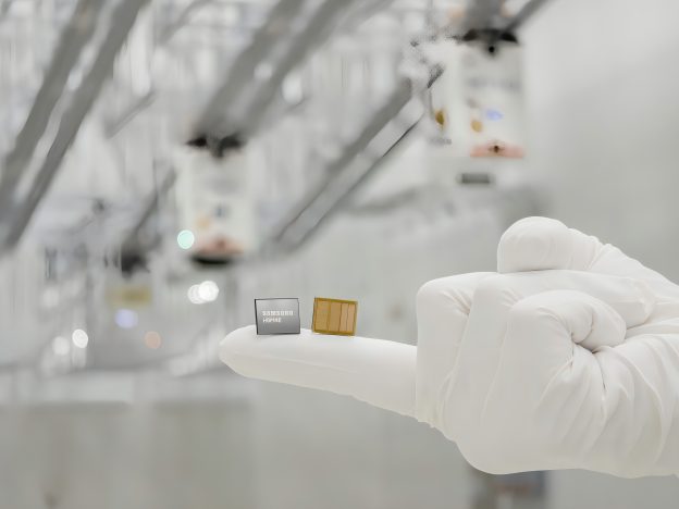
The thermal challenge is already shaping next-generation memory designs. According to Reuters, Samsung’s zHBM stacks memory vertically above AI accelerators, with its wafer-bonding technology expected to deliver over 10× the memory density of HBM5, 3× the energy efficiency, and more than 50% lower thermal resistance.
Beyond memory, rising AI chip power is putting further pressure on cooling systems. TrendForce notes that thermal design power (TDP) for individual AI chips from NVIDIA, AMD, and Google has surpassed 1 kW, while rack-scale systems now consume hundreds of kilowatts. Liquid cooling penetration among AI chips is projected to rise from around 33% in 2025 to 53% in 2026 and approach 60% in 2027.
CPO and STCO May Hold the Key to AI’s Thermal Challenge
Seoul National University of Science and Technology Professor Kim Sung-dong also identified thermal management as a major challenge for advanced semiconductor packaging. As highlighted by ETNews, Kim noted that the AI industry is increasingly prioritizing thermal management over further performance gains, pointing to co-packaged optics (CPO) and system-technology co-optimization (STCO) as key approaches. He added that the industry is accelerating technology development and commercialization efforts around STCO.
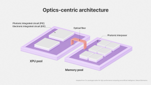
CPO converts electrical signals into optical signals, improving performance and power efficiency while reducing heat generation compared with conventional copper-based interconnects. STCO, meanwhile, aims to optimize overall system performance, including thermal management, the report notes.
Meanwhile, the ETNews report also notes that Professor Kim said the shift from basic data analysis and supporting simulations toward AI-driven digital twins is accelerating. He added that physics-informed neural networks (PINNs) and deep reinforcement learning are rapidly emerging as tools to autonomously design and optimize substrate warpage and power delivery networks (PDNs).
Read more
- Liquid Cooling Becomes Standard for High-End AI Infrastructure, with Penetration Expected to Reach 53% in 2026, Says TrendForce
- [News] Samsung, SK hynix Plan New Heat Dissipation Technologies Starting HBM5: Three Memory Makers’ Approaches in Focus
(Photo credit: Samsung)