


[News] Intel and Memory: A History of Exits, and a New Bid to Return
In a TechSurge podcast released last week, Intel CEO Lip-Bu Tan signaled the chip giant’s growing interest in memory, saying the company does not intend to miss the next major wave. As Intel explores technologies such as cross-batch memory (XBM) and Z-angle memory (ZAM), it is worth looking back at the company’s long and often bumpy history in memory—a sector where Intel has made several bold bets, with mixed results.
From DRAM Pioneer to Exit
Intel once had a foothold in both DRAM and NAND. As reported by EE Times, Team Blue launched the industry’s first commercial SRAM, the 3101, in 1969, followed by its first commercial DRAM, the 1103, a year later.
But by the early 1980s, Japanese rivals NEC, Hitachi and Fujitsu had gained a major manufacturing edge, achieving yields up to 40% higher than their U.S. counterparts while driving costs lower, EE Times suggests, adding that facing mounting losses and falling DRAM prices, Intel exited the business in 1985.
In a farewell letter posted on Intel’s website, the company noted that global capacity was driving prices to “unacceptable levels.” “With 256K DRAMs now selling at less than $3.00, it seems unlikely that we would attain an acceptable level of profitability in higher density products,” Intel said.
By the time Intel pulled the plug, DRAM accounted for less than 5% of its business, while the company expected “substantial losses” to continue through 1985 and beyond.
Intel’s memory ambitions did not end with its 1985 DRAM exit. In the late 1990s, the company made another bet on memory, backing Rambus’s RDRAM (Rambus Dynamic Random-Access Memory) for its Pentium 4 processors, EE Times reports. But RDRAM’s higher cost and latency failed to gain market traction, and Intel eventually abandoned the initiative in 2001, the report adds.
From NAND to Optane
Intel also entered the NAND market through its partnership with Micron. As previously reported by Commercial Times, the two companies formed the IMFT joint venture in 2006 to develop and manufacture NAND flash. By 2015, they had completed development of 3D XPoint and begun mass-producing 3D NAND.
Jointly developed by Intel and Micron, 3D XPoint was designed to deliver nonvolatile memory speeds up to 1,000 times faster than NAND flash, while its proprietary material and cross-point architecture could provide up to 10 times the density of conventional memory, according to Commercial Times.
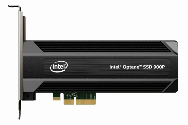
Intel later brought 3D XPoint to market through its Optane memory in 2017. However, the technology struggled to gain traction as alternatives such as HBM and multilayer 3D-stacked memory offered a stronger mix of performance, cost and scalability, according to EE Times. Optane ultimately failed to live up to expectations, leading Intel to discontinue the technology in 2022, the report adds.
As Intel doubled down on NAND, it also announced plans in 2015 to manufacture 3D NAND in China, sending a jolt through the flash market, as reported by The Register. But the NAND push ultimately lost momentum. Weak market adoption and mounting losses led Intel to sell its NAND business to SK hynix for $9 billion in 2020, as noted by EE Times.
Intel’s Next Memory Move: XHBM, ZAM
As highlighted by Tom’s Hardware, Intel’s latest memory push appears to focus on stacking memory atop CPUs and rethinking memory architecture—an ambition reflected in its XBM and Z-angle memory (ZAM) efforts.
Intel’s latest patent offers a closer look at XBM (cross-batch memory), which pairs a DRAM block with a 32 GT/s UCIe I/O block. Designed to match HBM4’s footprint, each XBM unit could pack 0.5–5.0GB of die capacity, with I/O routed through the base die, according to Wccftech.
XBM also takes a different path from conventional HBM. Rather than using a silicon interposer to connect memory to the host processor, it moves data over UCIe links, according to EE Times. At the cell level, XBM shifts the 1T1C memory cells from the front-end silicon into the back-end-of-line (BEOL), freeing front-end space for additional through-silicon vias (TSVs) and potentially enabling denser memory connectivity, the report adds.
Meanwhile, ZAM, which Intel is co-developing with SoftBank subsidiary SAIMEMORY, takes a different approach. The architecture uses fusion bonding to build a nine-layer stack of largely conventional DRAM, with silicon layers just 3 µm thick separating each tier. Intel is targeting roughly twice the bandwidth density of HBM4, according to EE Times.
The two technologies are still some distance from the market, with XBM expected to target commercialization after 2030, around the same timeframe as ZAM, according to Wccftech. Whether Intel can turn this ambitious memory blueprint into a commercial reality—and regain a meaningful foothold in memory—could become much clearer over the next two to three years.
Read more
- [News] Intel Patent Reveals XBM Matching HBM4 Footprint Without Interposers; Commercialization Seen After 2030
- [News] Intel, SoftBank Reportedly to Unveil ZAM-Based HB3DM in June, Bandwidth More Than Double HBM4
(Photo credit: Intel)


