[News] TSMC and Researchers Overcome 2D Semiconductor Bottleneck with Epitaxial Interface Engineering
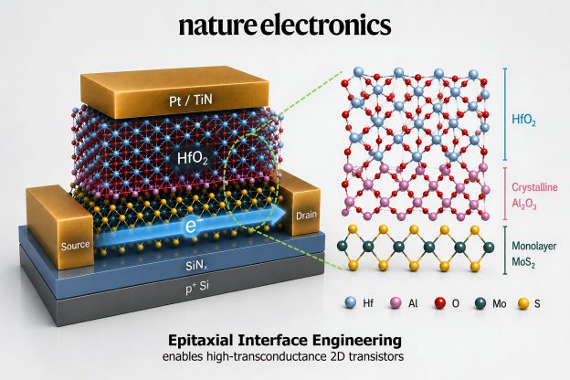
As conventional silicon semiconductor technology approaches its physical limits, 2D semiconductors are increasingly viewed as a key enabler for extending Moore’s Law. According to TechNews, citing Taiwan’s National Science and Technology Council (NSTC), a research team led by Dr. Iuliana Radu of TSMC, in collaboration with National Yang Ming Chiao Tung University (NYCU), has developed a high-performance monolayer molybdenum disulfide (MoS₂) top-gate transistor by addressing the long-standing interface challenges facing 2D semiconductors. The study was published in Nature Electronics.
The report explains that as silicon transistors approach their physical scaling limits, shrinking channel dimensions lead to higher leakage current and weaker electrostatic control. This has driven researchers to explore alternatives, with monolayer MoS₂ emerging as one of the most promising 2D semiconductor candidates. Despite its atomically thin structure, it retains semiconductor properties, making it well suited for smaller, more power-efficient transistors. However, 2D semiconductors require an ultrathin gate dielectric to control current flow, and depositing this layer often introduces dielectric-related scattering that degrades electron transport and device performance.
To overcome this challenge, the researchers focused not on discovering a new material, but on redesigning the interface through epitaxial interface engineering. Using ultra-high vacuum technology, the team first deposited an ultrathin aluminum layer onto monolayer MoS₂, then oxidized it to form an approximately 0.42nm-thick aluminum oxide (Al₂O₃) layer as a high-quality template for subsequent material growth. According to the report, this atomically thin interface improves the quality of the interface between the 2D semiconductor and the gate dielectric while reducing electron scattering, enabling both an ultrathin structure and high transconductance.
The resulting high-performance monolayer MoS₂ top-gate transistor delivers ultralow leakage current and excellent operational stability even at extremely small dimensions, the report says. By reconciling two long-standing tradeoffs—an ultrathin dielectric layer and high carrier mobility—the work demonstrates the practical potential of 2D semiconductor devices. According to the report, the technology could enable faster, lower-power electronic devices while integrating seamlessly with existing semiconductor manufacturing processes.
Leading Chipmakers Pursue 2D Transistor Technologies
TSMC has been advancing 2D-material transistor development. In June, TSMC, imec, and ASML unveiled a scalable 300mm integration route for 2D-material-based n-type field-effect transistors (nFETs) and p-type field-effect transistors (pFETs). According to an imec press release, the collaboration demonstrated, for the first time, 50nm contacted poly pitch (CPP) transistors using MoS₂, WS₂, and WSe₂ channel materials, establishing a manufacturing-compatible integration approach for next-generation 2D transistors.
Intel has also been advancing 2D transistor research. According to Tom’s Hardware, Intel Foundry and imec demonstrated a 300mm-ready integration of key process modules for 2D field-effect transistors (2DFETs) in late 2025. The collaboration featured a fab-compatible contact and gate-stack integration scheme, marking another step toward future manufacturing of 2D-material-based transistors. While commercialization remains a long-term goal, the work helps de-risk the development and eventual production of chips based on 2D materials.
Read more
- [News] imec Roadmap Extends to A3 by 2038; Chip Density Gains Shift Beyond Traditional Transistor Scaling
- [News] TSMC’s 1.4nm Fab Ahead of Schedule; First Building Expected Before Apr. 2027, Mass Production Seen by Mid-2028
(Photo credit: National Science and Technology Council)