


[News] imec Roadmap Extends to A3 by 2038; Chip Density Gains Shift Beyond Traditional Transistor Scaling
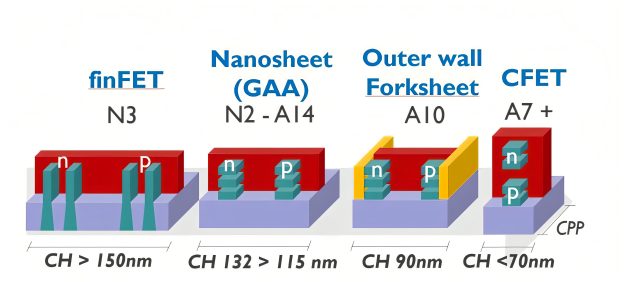
Leading semiconductor research institute imec has unveiled its latest process roadmap, signaling a major shift in the evolution of advanced chips. According to TechNews, citing Tom’s Hardware, the roadmap suggests that traditional transistor scaling will no longer be the sole driver of chip density as contacted poly pitch (CPP) approaches its practical limits.
imec forecasts that semiconductor technology will advance to the A3 (0.3nm) generation by 2038. However, after the A10 (~1nm) generation, expected around 2030, further scaling of CPP is expected to face fundamental limitations, meaning future gains in chip density will increasingly depend on reducing standard cell height alongside new device architectures and advanced integration technologies.
From Transistor Scaling to New Density Drivers
As the report notes, the roadmap projects the A14 node to arrive in 2028, with CPP shrinking to around 45nm and standard cell height falling to about 115nm. High-NA EUV is also expected to be introduced at this stage. From the A10 to A5 generations, however, CPP is projected to remain at roughly 42nm, suggesting traditional transistor scaling alone will no longer deliver meaningful gains in chip density.
Against this backdrop, Tom’s Hardware notes that imec’s roadmap identifies A7 as the likely starting point for CFET. However, because A7 retains the same 42nm CPP as A10, the report notes that adoption of the new transistor architecture at this node remains uncertain. It also points out that imec appears to regard back-side power delivery networks (BSPDN) as a prerequisite for CFET.
The roadmap continues to evolve beyond A7. According to Tom’s Hardware, the A5 generation, expected in 2035–2036, maintains a 42nm CPP while reducing standard cell height to around 64nm. By 2038, the roadmap reaches the A3 generation with a 39nm CPP and a 50nm standard cell height. At that point, imec envisions a progression from sequential to bonded CFET implementations to further leverage vertical integration. The report adds that achieving the A3 targets may also require Hyper-NA EUV lithography.
Economic Daily News also notes that CFET is expected to become the next mainstream transistor architecture after FinFET and gate-all-around (GAA), replacing the conventional side-by-side layout by vertically stacking n-type and p-type transistors. The report also says TSMC has demonstrated a CFET ring oscillator comprising around 1,000 transistors.
Read more
- [News] TSMC Latest Roadmap: A12, A13 for 2029 Without High-NA EUV; A16 Volume Production Delayed to 2027
- [News] Intel Reportedly Weighs Dual-Side Power Delivery for 14A2 to Boost Chip Density in Race With TSMC, Samsung
(Photo credit: imec)


