[News] TSMC’s Taichung 1.4nm P1, P2 Fabs Could Begin Mass Production in 2027, Ahead of 2028 Plan
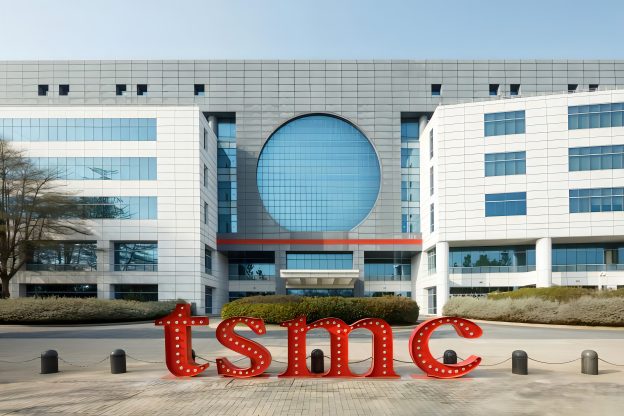
TSMC is making steady progress on the second-phase expansion of its Central Taiwan Science Park site in Taichung. According to Commercial Times, Central Taiwan Science Park Administration Deputy Director-General Wang Chun-chieh said on September 9 that the expansion site is planned to house four 1.4nm fabs. P1 is currently undergoing floor-slab construction and is expected to be completed and enter production in April 2027, while P2 is undergoing foundation construction and is scheduled for completion in October 2027. Notably, Economic Daily News adds that P1 could begin mass production as early as 2H27, well ahead of the original plan to begin mass production in 2028.
As for the subsequent phases, Commercial Times notes that P3 has already secured a construction permit, while P4’s permit application is still underway. The report notes that all four fabs are expected to be completed by 2028. Economic Daily News also indicates that P3 is scheduled for completion in 2Q28, followed by P4 in 4Q28.
Regarding the potential revenue, Economic Daily News notes that the Central Taiwan Science Park Administration previously estimated annual revenue of NT$500 billion once TSMC’s 1.4nm fabs are completed and enter mass production. However, the administration said a more accurate estimate will have to wait until production capacity at TSMC’s second Baoshan fab in the Hsinchu Science Park becomes clearer. Based on current manufacturing costs and market demand, it said the NT$500 billion estimate “may be an underestimate.”
TSMC Expansion Spurs Supplier Cluster in Taichung
The ripple effects of TSMC’s expansion in Central Taiwan Science Park have continued to grow in recent years. According to Economic Daily News, leading semiconductor equipment suppliers, including lithography giant ASML, Japanese chip equipment maker Tokyo Electron (TEL), and U.S. process control and yield management leader KLA, have all established operations in Taichung’s 7th Redevelopment Zone to be closer to TSMC.
The report also notes that TSMC has recently been rumored to be considering the acquisition of AUO’s L7 and L5C facilities in Central Taiwan Science Park, located near its Fab 15 site. The move would help prepare for the large-format optoelectronic integration capabilities required for future co-packaged optics (CPO) applications.
TSMC Moves Ahead on 1.4nm as Intel Targets 2028, Samsung 2029
Meanwhile, Samsung Foundry has recently revised the mass-production timeline for its 1.4nm process. As Economic Daily News notes, Samsung had initially targeted 2027 for 1.4nm mass production but updated its technology roadmap, pushing the target to 2029. The report notes that the revised schedule would put Samsung behind foundry leader TSMC’s A14 timeline. As for another key player in the foundry market, a Tom’s Hardware report from June notes that Intel plans to begin mass production using its 14A (1.4nm-class) technology in 2028.
Read more
- [News] Intel CFO Says 14A Defect Reduction Fastest Since 22nm; Customer Talks Reportedly Grow Ahead of 2028 Ramp
- [News] TSMC Equipment Demand Reportedly Jumps 90% in Just Over Half a Year; Substrate Capacity Faces AI Squeeze
(Photo credit: TSMC)