[News] Samsung Reportedly Expands 2nm Portfolio Ahead of 2029 SF1.4 Mass Production; SF2P+ Targets 2027–28
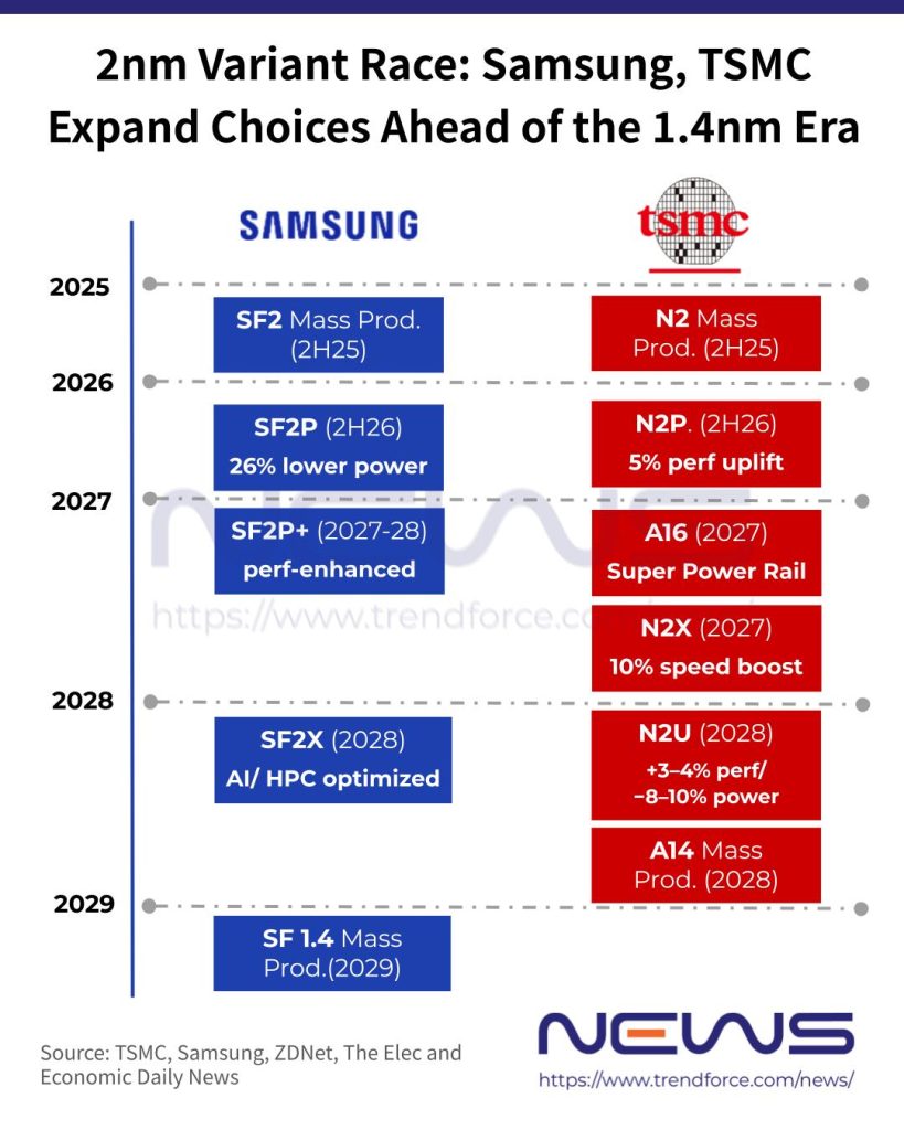
As leading foundries now target 2028–29 for 1.4nm-class mass production, they are accelerating enhanced 2nm variants to bridge the gap, giving customers more options as manufacturing costs continue to climb. According to ZDNet, Samsung Foundry’s SF1.4 is now reportedly slated for mass production in 2029, while its 2nm performance-enhanced variant, SF2P+, is expected to arrive earlier, between 2027 and 2028.
Against this backdrop, Samsung is expanding its 2nm roadmap. Citing Shin Jong-shin, Vice President of Samsung Foundry’s Design Platform Development Team, The Elec reports that the platform will evolve from SF2 and SF2P to the performance-enhanced SF2P+, before advancing to SF2X.
SF2P+ is reportedly targeted for mass production between 2027 and 2028, while SF2X will follow as a next-generation node optimized for artificial intelligence (AI) and high-performance computing (HPC) workloads, according to The Elec.
Highlighting the roadmap’s benefits, Shin said the transition from SF2 to SF2P cuts power consumption by 26% while boosting operating frequency by 15%, with more than half of those gains driven by DTCO (design-technology co-optimization), the report adds.
Looking beyond SF1.4, Samsung is also developing an enhanced SF1.4+ node, which ZDNet reported is scheduled to debut in 2030 with further improvements in yield and performance.
TSMC Builds Out Its 2nm-Class Node Portfolio
On the other hand, TSMC is also expanding its 2nm-class roadmap to better address growing customer demand. While the company’s most advanced node currently stands at 2nm, built on first-generation nanosheet transistor technology, the N2P process is expected to enter mass production in the second half of this year, while the N2X and N2U variants are scheduled to follow in 2027 and 2028, according to the Economic Daily News.
As explained by a previous Tom’s Hardware report, TSMC’s N2U is positioned as a third-year enhancement of the N2 platform, leveraging DTCO (Design-Technology Co-Optimization) to deliver incremental but meaningful gains—approximately 3% to 4% higher performance at the same power level, or 8% to 10% lower power consumption at the same operating speed, along with a modest 2% to 3% improvement in logic density.
Notably, the node maintains full compatibility with N2P IP, enabling customers—particularly in the client computing segment—to develop next-generation products without migrating to an entirely new process node, thereby avoiding substantial redesign costs, Tom’s Hardware reports.
Meanwhile, the A16 process featuring Super Power Rail (SPR) is expected to be production-ready in the second half of this year, although it is officially positioned as a 2027 node, the report adds.
Read more
- [News] Samsung Foundry Reportedly in Talks With Chinese Carmakers Like BYD for 2nm, 4nm Autonomous Driving SoCs
- [News] Samsung Reportedly in Talks for Google 2nm TPU I/O Die Order; 2028 Mass Production Eyed
(Photo credit: Samsung)