[News] SK Group Chair Chey Tae-won Meets TSMC Chairman C.C. Wei After Two Years, HBM, Advanced Packaging in Focus
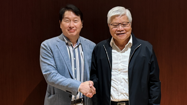
Shortly after touring SK hynix’s COMPUTEX booth in Taipei alongside NVIDIA CEO Jensen Huang on June 2, SK Group Chairman Chey Tae-won met with TSMC Chairman C.C. Wei for the first time in two years, according to a post by SK hynix on its official X account on June 4. Hankyung adds that the meeting marked their first encounter since June 2024.
As highlighted by SK hynix, the meeting centered on next-generation AI technologies, HBM, and advanced packaging, highlighting the growing need for deeper collaboration across the AI value chain.
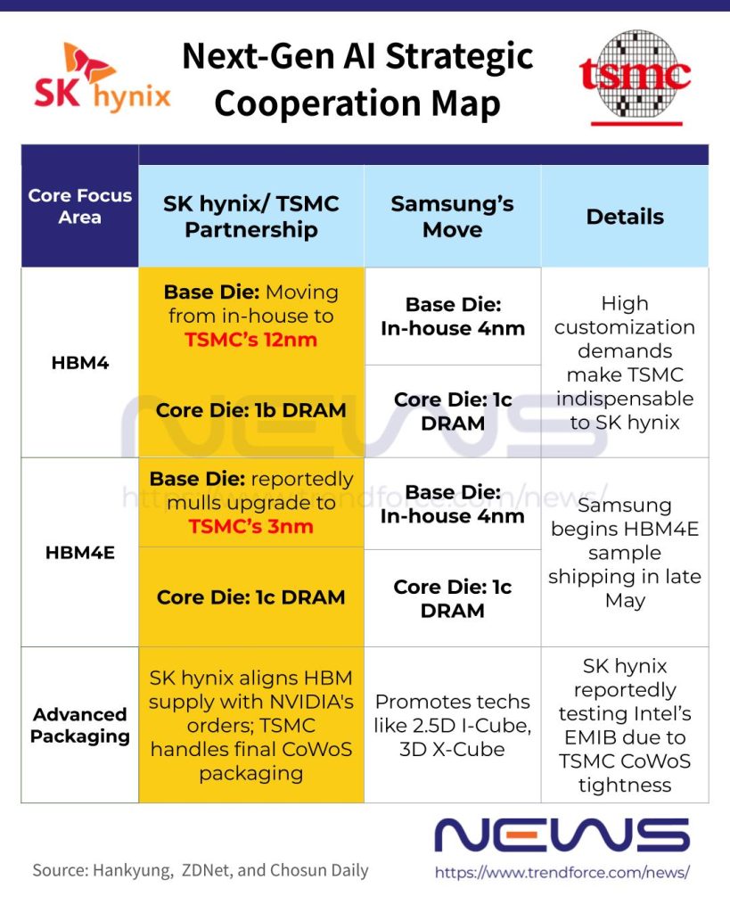
Hankyung points out that the partnership between SK hynix and TSMC is also closely tied to NVIDIA’s upcoming AI accelerator roadmap. HBM4, SK hynix’s sixth-generation HBM set to power NVIDIA’s next-generation Vera Rubin platform, combines a 12nm base die manufactured by TSMC with SK hynix’s fifth-generation 10nm-class (1b) DRAM process, the report suggests.
Notably, Chosun Daily explains that TSMC, the world’s leading pure-play foundry, has become a key HBM partner for SK hynix amid a structural shift in base die production: up to its HBM3E generation, SK hynix produced base dies in-house. However, starting with HBM4, production has been outsourced to TSMC.
The report attributes the shift to growing customer demand for greater customization of base-die functionality, with SK hynix leveraging TSMC’s advanced process capabilities to enable more precise feature implementation.
Against this backdrop, a separate Chosun Daily report in March also noted that SK hynix is considering TSMC’s 3nm for its HBM4E logic dies, as it seeks to compete with Samsung’s planned use of its in-house 4nm process for HBM4E logic dies.
CoWoS Capacity Tightness Puts Advanced Packaging in Focus
Meanwhile, advanced packaging has emerged as another key bottleneck in the AI era, and was also a focal point of the discussions between TSMC and SK hynix. According to EToday, SK hynix currently operates a closely integrated collaboration framework with NVIDIA and TSMC, under which HBM supply is aligned with NVIDIA’s orders, while TSMC is responsible for advanced packaging.
Maeli Business further notes that the chip-on-wafer-on-substrate (CoWoS) process, a key advanced packaging technology for AI semiconductors that integrates GPUs and HBM into a single package, is currently unable to keep pace with surging demand. To meet soaring demand, TechNews previously reported that TSMC’s CoWoS capacity is expected to reach around 115,000 to 140,000 wafers per month by the end of 2026, and further increase to approximately 170,000 wafers per month in 2027.
However, amid ongoing capacity tightness at TSMC, ZDNet reported that SK hynix is also exploring collaboration with Intel in advanced packaging, reportedly testing Intel’s EMIB-based 2.5D packaging for HBM applications.
Read more
- [News] SK hynix Introduces iHBM Solution, Targets HBM5 Adoption with 30% Thermal Resistance Reduction
- [News] SK hynix Reportedly Tests Intel EMIB 2.5D Packaging With HBM Amid TSMC CoWoS Tightness
(Photo credit: SK hynix’s X)


