[News] Behind TSMC’s High-NA EUV Deferral: Low-NA Stays Strong, Customer Landscape Shifts, and ASML Quietly Pivots
One of the most closely watched issues in the semiconductor equipment space lately is TSMC’s statement that it does not plan to adopt High-NA EUV systems for its A13 node, scheduled around 2029. The move has sparked debate over whether—and to what extent—this decision could impact ASML’s future growth trajectory.
Against this backdrop, the implications extend beyond ASML’s product roadmap, shaping both customer adoption strategies and near-term EUV demand outlook.
High-NA EUV: Too Costly for Near-Term Adoption?
Even for a foundry leader projecting up to $560 billion in capital expenditure for 2026, ASML’s High-NA EUV systems are still viewed as expensive, with each tool priced at around $400 million—roughly double the cost of current-generation EUV systems, according to Reuters, a consideration that becomes more pronounced as TSMC accelerates capacity expansion across new fabs in the U.S., Japan and other overseas sites.
In this context, TSMC’s decision to defer High-NA EUV adoption reflects a broader strategy of extending the performance envelope of existing Low-NA EUV tools. Kevin Zhang, deputy co-chief operating officer and senior vice president at TSMC, told Reuters that the company’s R&D has been “exceptionally effective” in pushing current EUV capabilities while still maintaining an aggressive scaling roadmap.
In line with this strategy, TSMC expanded its 1–2nm roadmap at its North America Technology Symposium last week with several node variations designed to improve efficiency without requiring a shift to next-generation lithography. As reported by Tom’s Hardware, these include the 1.2nm- and 1.3nm-class nodes A12 and A13, along with an unexpected extension of the N2 family under the N2U label, targeting between 2028 and 2029.
Low-NA EUV Extends Scaling Path
TSMC noted that A13 is derived from A14 through an optical shrink, delivering around a 6% reduction in die area while maintaining full design-rule and electrical compatibility, allowing customers to upgrade with minimal redesign effort. As highlighted by Micro Electronics, this also enables direct reuse of existing IP, suggesting such incremental scaling can still be efficiently supported by Low-NA EUV combined with multi-patterning techniques.
TechPowerUp explains that Low-NA EUV multi-patterning involves multiple exposure passes to define a single layer, with two etching runs effectively replicating some benefits of High-NA exposure. However, the report adds the technique becomes increasingly constrained at advanced nodes approaching 1nm and below, where High-NA EUV is expected to become necessary.
As a result, Low-NA EUV remains sufficient for TSMC’s near-term roadmap. Thus, the foundry giant—supported by strong demand for its 3nm and 2nm—appears in no rush to commit to High-NA EUV adoption, opting instead to monitor how the transition unfolds among peers. As previously reported by Reuters, ASML customers, including Intel and SK hynix, are already preparing to adopt High-NA EUV systems as early as 2027, targeting next-generation AI logic and high-bandwidth memory chips.
ASML Sees Low-NA EUV Demand Strong
Notably, ASML—echoing TSMC’s stance—continues to see strong momentum in Low-NA EUVs. According to an Investing.com transcript, CFO Roger Dassen indicated the company is targeting at least 60 Low-NA EUV systems in 2026, with plans to scale that further to around 80 in 2027. For context, Chosun Daily notes that ASML typically produces only around 40–50 systems per year.
Interestingly, while ASML did not disclose High-NA EUV shipment targets or detailed revenue breakdowns, it still offered partial visibility into the segment. According to the transcript, the company reported net system sales of €6.3 billion in 1Q26, with EUV systems contributing more than €4.1 billion, including revenue from two High-NA units.
Assuming an external benchmark of roughly $400 million per High-NA tool, this would imply that the bulk of ASML’s EUV revenue still came from Low-NA systems.
In the meantime, ASML also underscored the extended lifecycle of its Low-NA EUV platform. The company, at the earnings call, pointed to its 1,000-watt light source demonstration as a key milestone, enabling long-term scalability. It noted that by 2031, Low-NA EUV tools are expected to reach 330 wafers per hour—significantly higher than current performance levels—reinforcing their role as the workhorse of EUV manufacturing for many years ahead.
New Momentum Beyond EUV
Against the backdrop of uncertainty over next-gen EUV demand, the Dutch equipment maker is also looking to move beyond its lithography core, targeting expansion into advanced packaging, according to a March Reuters report.
The Elec further reports that ASML is believed to be advancing wafer-to-wafer (W2W) hybrid bonding equipment, based on a patent analysis presented at an industry conference. The findings suggest the company is drawing on its core Twinscan lithography platform expertise as it explores development of a W2W hybrid bonder.
Notably, industry expectations point to Samsung and SK hynix potentially adopting hybrid bonding at the latest in HBM5, which could open a new long-term growth driver for ASML.
Who Remains ASML’s Largest Customer?
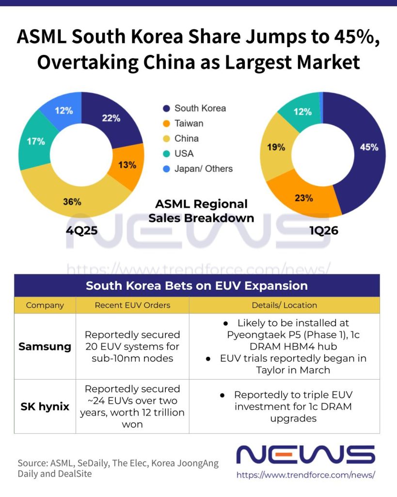
TSMC has long been regarded as ASML’s largest customer. Common Wealth Magazine previously reported that the company accounted for 56% of the global installed EUV base. A 2024 South China Morning Post report, citing AnandTech and The Register, further noted that TSMC’s share of global EUV system installations increased from 50% in 2020 to 56% in 2023.
This dominance, however, is increasingly being viewed through a historical lens. As memory manufacturers significantly ramp up capital expenditure to support the AI-driven HBM cycle, the composition of ASML’s top customer base is gradually shifting.
Notably, ASML has already seen a sharp increase in South Korean demand, with the region accounting for 45% of its 1Q26 sales, up from 22% in 4Q25. According to SeDaily, Samsung is also expanding its lithography capacity through large-scale equipment orders, securing around 20 EUV systems from ASML for sub-10nm advanced process nodes.
At the same time, TSMC’s growing role in advanced packaging highlights its broader technology diversification beyond traditional foundry services. Against this backdrop, ASML’s revenue exposure may gradually shift toward a more diversified customer base.
Whether TSMC’s incremental scaling strategy can outperform the more aggressive High-NA adoption approach taken by peers, and whether ASML can successfully navigate this technological transition, remains one of the semiconductor industry’s most closely watched dynamics.
Read more
- [News] TSMC Latest Roadmap: A12, A13 for 2029 Without High-NA EUV; A16 Volume Production Delayed to 2027
- [News] ASML Raises 2026 Sales Outlook to €36B–€40B on Memory, Logic Demand; South Korea Share Hits 45%
(Photo credit: ASML)