[News] Intel Launched World’s First Thinnest GaN Chiplet
On April 9, Intel Foundry Services announced a major technological breakthrough with the development of the world’s thinnest gallium nitride (GaN) chiplet. The silicon substrate has been reduced to just 19 micrometers—approx. one-fifth the diameter of a human hair.
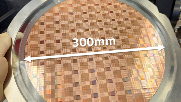
The chiplet is fabricated on a 300 mm (12-inch) GaN-on-silicon wafer using Intel’s proprietary stealth dicing and thinning process. This approach enables ultra-thin form factors while maintaining structural integrity and performance stability.
More notably, the team has, for the first time, achieved monolithic integration of GaN power transistors with silicon-based digital logic circuits. By embedding complex computing functions directly into the power chiplet, the design eliminates the need for additional auxiliary chips, significantly simplifying system architecture and reducing inter-component energy loss.
Performance tests show that the GaN transistors can withstand voltages up to 78 V and achieve a radio-frequency cutoff exceeding 300 GHz, meeting the demands of high-frequency communication applications. The integrated digital logic library operates reliably, with inverter switching speeds as fast as 33 picoseconds and consistent performance across the entire wafer, indicating strong potential for mass production. The technology has also passed four industry-standard reliability tests, demonstrating its capability to operate under high-temperature and high-voltage conditions, and meeting commercial deployment requirements.
As traditional silicon-based technologies approach their physical limits in high-power and high-frequency scenarios, GaN—recognized as a wide bandgap semiconductor—offers advantages such as higher power density, faster switching speeds, and lower energy consumption.
By leveraging 300mm GaN-on-silicon wafer processing, Intel’s solution is compatible with existing semiconductor manufacturing infrastructure, which could significantly reduce production costs and accelerate large-scale adoption.
(Photo credit: Intel)


