[News] TSMC Advances Panel-Level Packaging, CoPoS Pilot Line Reportedly Set for June Completion, 2028–29 Ramp Eyed
Ahead of TSMC’s earnings call later this week, the spotlight is once again on its advanced packaging roadmap—and CoWoS is no longer the only story. According to Commercial Times, TSMC’s CoPoS (Chip-on-Panel-on-Substrate) pilot line has already begun tool deliveries to R&D teams in February, with the full line on track for completion by June.
Commercial Times notes that the rise of CoPoS underscores an industry shift toward panelization as a key solution to advanced packaging bottlenecks: as AI chip reticle sizes continue to expand—such as NVIDIA’s Rubin GPU reaching 5.5x—a standard 12-inch wafer can now accommodate just 7, or in some cases as few as 4, units. Square panel formats, as per the report, offer a step-change in utilization and throughput, with the longer-term goal of replacing silicon interposers with glass substrates.
With TSMC’s CoPoS pilot line set for completion by mid-year, the industry broadly expects volume production to ramp between 2028 and 2029, according to Commercial Times. However, supply chain sources cited by the report also caution that as substrate sizes expand, warpage issues intensify in tandem, emerging as one of the biggest hurdles to mass production.
Chiayi Emerging as Key CoPoS Hub
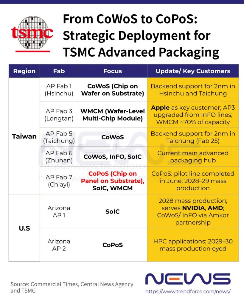
Meanwhile, Central News Agency notes that TSMC may establish its first CoPoS pilot line in Chiayi, with potential production planned at the site, which is further expected to integrate CoPoS, SoIC (System on Integrated Chips), and WMCM (Wafer-Level Multi-Chip Module) capabilities.
Central News Agency suggests that TSMC is also planning to convert existing 8-inch fabs in Taiwan into advanced packaging facilities, while current backend sites will support 2nm leading-edge production.
The report further outlines a clearer roadmap for TSMC’s advanced packaging network in Taiwan. Institutional analysis suggests Advanced Packaging Fab 1 in Hsinchu will support 2nm-related packaging for both Hsinchu and Taichung production bases, while Longtan Advanced Packaging Fab 3 is mainly dedicated to wafer-level multi-chip module (WMCM) and InFO solutions for high-end processors from Apple.
Meanwhile, Central News Agency notes that TSMC’s Advanced Packaging Fab 5 in Taichung is expected to support 2nm output from Fab 25, while Fab 6 in Zhunan, Miaoli integrates SoIC, InFO, CoWoS, and advanced testing capabilities, with SoIC serving as the core capacity driver.
TSMC’s mid-January earnings call outlined a 2026 capital expenditure plan of $52 billion to $56 billion. According to Central News Agency, around 70%–80% will go to advanced process technologies, about 10% to specialty nodes, and another 10%–20% to advanced packaging, testing, mask production, and related areas.
The report adds that advanced packaging accounted for roughly 8% of TSMC’s revenue in 2025, and is expected to surpass 10% in 2026.
U.S. Advanced Packaging Ramps in Sync
TSMC’s advanced packaging capacity in the U.S. is also ramping up. According to Economic Daily News, the company’s upcoming third U.S. fab capacity is already largely booked through 2027, implying that output coming online between 2027 and 2029 has effectively been secured in advance by customers.
With leading-edge wafer capacity in the U.S. fully reserved over the next three years, TSMC’s advanced packaging must scale in tandem to ensure seamless, just-in-time delivery. Market analysis cited by Central News Agency highlights sustained CoWoS demand from NVIDIA and AMD, while Apple continues to rely on InFO for its high-end processors. AMD is also a key SoIC customer, reinforcing TSMC’s push to expand advanced packaging capacity in the U.S. to serve major American clients.
According to Central News Agency, citing institutional and supply chain sources, TSMC’s first advanced packaging facility in Arizona will enter volume production in 2028, followed by a second site ramping between 2029 and 2030, primarily focused on SoIC and CoPoS lines.
Read more
(Photo credit: TSMC)


