[News] JEDEC Reportedly Plans to Relax HBM Height Specs to ~900µm, Potentially Slowing Hybrid Bonding Adoption
JEDEC is reportedly considering relaxing standards governing next-generation HBM. According to Chosun Ilbo, sources indicate that JEDEC (Joint Electron Device Engineering Council) is weighing a plan to raise HBM height specifications to around 900 micrometers (µm).
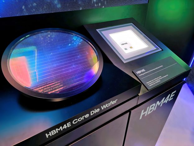
As reported by Newsis, the new standards are expected to take effect starting with seventh-generation HBM4E. For reference, the height specification is about 720 µm for fifth-generation HBM3E and around 775 µm for sixth-generation HBM4, underscoring a notable relaxation.
Industry observers cited by Newsis say easing the standards may help relieve production bottlenecks for memory makers and support faster mass production of next-generation products. The need to process ultra-thin DRAM wafers may decline, while error management during stacking could also become less complex.
Easing Standards May Reshape Hybrid Bonding Adoption and Competitive Landscape
At the same time, a significant relaxation of height standards could delay the adoption of hybrid bonders. As noted by Chosun Ilbo, with looser specifications, existing TC bonders may still support higher layer counts, allowing Hanmi Semiconductor, a dominant TC bonder supplier, to maintain its leading position.
Chosun Ilbo notes that scaling HBM to up to 20 layers will require thinner DRAM, pushing against technical limits. One solution is hybrid bonding equipment. While conventional thermocompression (TC) bonders connect layers using micro-bumps, hybrid bonders enable direct chip-to-chip bonding without bumps, reducing spacing and allowing more DRAM layers to be stacked within the same height constraints.
The hybrid bonding market is currently led by Netherlands-based BESI. In Korea, Hanwha Semitech plans to supply its second-generation hybrid bonder to customers in the first half of this year for performance testing, according to News Tomato.
Hybrid Bonding Adoption Hinges on Technology Readiness and Customer Demand
Still, as Chosun Ilbo notes, industry consensus holds that hybrid bonding will ultimately be unavoidable. Lee Kang-wook, Vice President of Package Development at SK hynix, said, as cited by Chosun Ilbo, that hybrid bonding will be essential for HBM stacks of 20 layers or more. The report adds that Samsung Electronics recently showcased its hybrid bonding technology at NVIDIA’s GTC 2026, claiming over 20% improvement in thermal resistance versus TC bonding and support for stacks exceeding 16 layers.
Meanwhile, Chosun Ilbo also notes that a key factor in adoption is major customer NVIDIA, as Samsung Electronics and SK hynix develop and supply HBM in line with its performance requirements.
Notably, according to The Elec, Samsung Electronics has begun introducing new inspection equipment for hybrid bonding. The company is discussing adoption and pursuing joint development with multiple vendors offering ultrasound- and X-ray-based non-destructive inspection technologies to detect micro-defects such as voids at hybrid bonding interfaces. Among the leading players is U.S.-based Onto Innovation, which has entered a joint development program (JDP) with Samsung and has already supplied equipment to mass production lines.
Read more
- [News] Industry Weigh 825–900 μm HBM Thickness for 20-High Stacks, Potentially Slowing Hybrid Bonding
- [News] While DDR5 Margins Reportedly Surpass HBM: What’s Next for Memory Giants?
(Photo credit: Samsung)


