[News] imec Secures ASML’s Most Advanced EXE:5200 High-NA EUV for Sub-2nm; 4Q26 Qualification Target
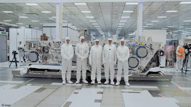
Belgian chip research institute imec announced that it has received an ASML tool that could advance next-generation chipmaking. According to its press release, imec has taken delivery of ASML EXE:5200 High-NA EUV system—the most advanced lithography tool available today. The system is expected to give imec’s global partner ecosystem early access to advanced chipmaking technologies, supporting sub-2nm logic and high-density memory development. Reuters adds that the system costs roughly $400 million and is one of fewer than a dozen units worldwide.
Imec expects the EXE:5200 High-NA EUV lithography system to be fully qualified by Q4 2026, according to its press release. In the meantime, the joint ASML–imec High-NA EUV lab in Veldhoven will remain operational, ensuring continued R&D activities for imec and its ecosystem partners.
The acquisition of this system marks a key milestone in imec’s five-year strategic partnership with ASML, supported by the EU (Chips Joint Undertaking and IPCEI), as well as the Flemish and Dutch governments, as its press release indicates. Imec CEO Luc Van den hove stated that, as part of the EU-funded NanoIC pilot line, the tool is expected to play a pivotal role in strengthening Europe’s leadership in advanced semiconductor R&D in the decades ahead.
Chipmakers Begin Installing High-NA EUV Systems
Ahead of imec’s move, leading chipmakers had already started integrating High-NA EUV systems to prepare for next-generation production. In a late-2025 blog post, Intel said it had completed acceptance testing of ASML’s second-generation High-NA EUV system, the TWINSCAN EXE:5200B. Meanwhile, in September 2025, SK hynix installed the same system at its DRAM fab to prepare for mass production.
Korea Economic Daily also reported that Samsung is moving on a roughly parallel timeline, having received its first High-NA EUV scanner, the TWINSCAN EXE:5200B, in late 2025, with a second unit expected in the first half of 2026.
Meanwhile, according to Bloomberg, ASML CEO Christophe Fouquet expects high-volume manufacturing to begin in 2027 and 2028, with the company working alongside customers through 2026 to ensure the machines can operate with minimal downtime.
High NA refers to the system’s larger numerical aperture—similar to a camera—which enables the creation of chip features up to 66% smaller, improving both speed and energy efficiency, Reuters notes.
Beyond EUV: ASML Reportedly Eyes Hybrid Bonding
In addition to providing the most advanced lithography tool, ASML is reportedly expanding into advanced packaging through hybrid bonding. According to The Elec, sources say the company is developing a hybrid bonding system and has begun designing its overall architecture, targeting semiconductor back-end processes.
Read more
- [News] ASML’s High-NA EUV for 2027-28: Which Giants Are Betting Big—Intel, Samsung, SK hynix or TSMC?
- [News] Intel Completes First 2nd-Gen High-NA EUV Acceptance Testing; ASML Eyes 2027–28 Mass Production
(Photo credit: imec)


