[News] Samsung Reportedly Eyes 2nm Base Die for HBM5, 1d DRAM HBM5E; HBM4 to Exceed 50% of Output
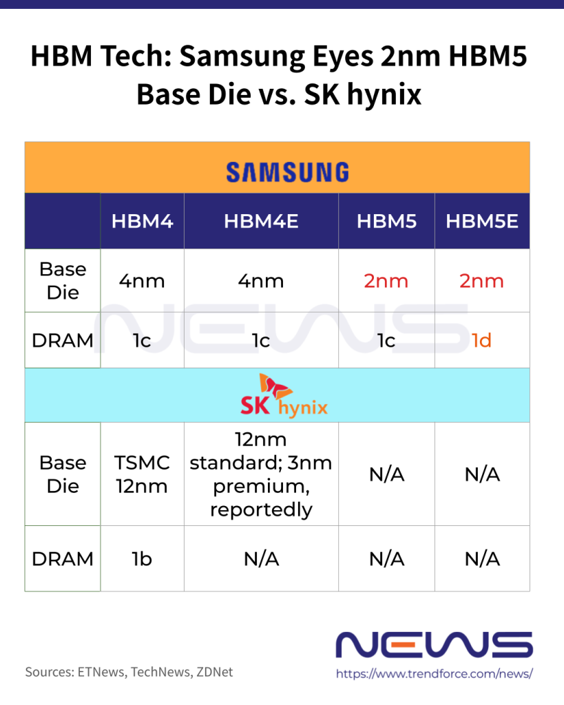
While HBM4 is only just entering mass production this year, Samsung is already looking ahead. According to ETNews, speaking at NVIDIA GTC, Hwang Sang-jun, Vice President and Head of Memory Development at Samsung Electronics, said that the base die of HBM5 will adopt Samsung Foundry’s 2nm process, compared with the 4nm base dies used in HBM4 and HBM4E.
Furthermore, as the report notes, Vice President Hwang said that 1d DRAM will be used as the core stacked memory in HBM5E, noting that although it increases costs, adopting leading-edge processes is unavoidable to meet HBM’s targeted performance. Meanwhile, its HBM4 and HBM4E use 1c DRAM, the report adds.
The report also notes that the 1d DRAM to be used in HBM5E is still under development at Samsung Electronics and has yet to be commercialized. However, sources cited in the report indicate that Samsung has already achieved strong performance and test yields for the technology.
In addition to outlining its next-generation roadmap, Vice President Hwang also addressed Samsung’s memory strategy. As Yonhap News indicates, Hwang said that the company aims for HBM4 to account for more than half of total HBM. Samsung Electronics plans to increase its production of HBM by more than threefold this year compared to last year, the report adds.
Samsung Expands Role in NVIDIA Ecosystem with Groq 3 Production
Meanwhile, according to Yonhap News, Hwang said the inference-focused chip “Groq 3,” for which NVIDIA CEO Jensen Huang has acknowledged Samsung’s contribution, is being produced at Samsung’s Pyeongtaek campus. Mass production is targeted between late 3Q and early 4Q this year, with orders already exceeding expectations.
Samsung’s Hwang Sang-jun also noted, according to the report, that Groq had been a customer of Samsung Foundry even before entering a licensing agreement with NVIDIA. Yonhap News adds that the Groq 3 chip features a large die exceeding 700 mm², allowing for only about 64 chips per wafer—significantly fewer than the typical 400–600. Around 70–80% of the chip is composed of SRAM, enabling fast on-chip inference without relying on external HBM.
As SEDaily highlights, Samsung’s production of the Groq 3 LPU chip is widely seen as positioning the company as a key partner across the full stack of next-generation AI accelerator platforms, following its foundry division’s entry into NVIDIA’s supply chain. Previously limited to supplying memory, Samsung has now expanded its role to include LPU manufacturing, further deepening the partnership.
Read more
- [News] Key GTC Takeaways: How Samsung, Micron, Intel & More Power NVIDIA’s Vera Rubin and Feynman
- [News] NVIDIA’s China-Ready LPUs Could Launch as Early as May; H200 Production Restarts
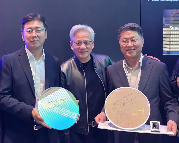
(Photo credit: Samsung)
Please note that this article cites information from ETNews, Yonhap News, and SEDaily.


