[News] NVIDIA Rubin Ultra and Feynman Reportedly to Boost TSMC SoIC; Besi, Applied Materials, TEL to Benefit
NVIDIA’s GTC revealed plans to launch an enhanced Rubin Ultra in 2027, while its next-generation architecture, Feynman, is also coming into view for 2028. According to Commercial Times, SoIC (System on Integrated Chips) is expected to be a key technology for TSMC to meet customer design needs for these future platforms. By vertically stacking dies, SoIC can significantly boost transistor density and help overcome the limitations of Moore’s Law. The report adds that Rubin Ultra will comprise seven chips and five rack configurations, while Feynman is expected to adopt customized HBM alongside higher-density chiplet designs.
As the report highlights, NVIDIA’s adoption of the Feynman architecture will mark a key turning point, with SoIC usage set to rise significantly. SoIC leverages copper-to-copper hybrid bonding to vertically stack multiple dies, enabling shorter interconnects and lower power consumption. Compared with mainstream 2.5D packaging such as CoWoS, SoIC offers higher bandwidth and better energy efficiency, making it well suited for next-generation AI chips.
Supply chain sources say TSMC plans to build monthly SoIC capacity of around 10,000 to 15,000 wafers by 2026, with further expansion to support demand from NVIDIA, Broadcom, and AMD from 2027 onward. Institutional investors indicate that SoIC requires significantly higher capital expenditure per unit than CoWoS, with investment reaching about $6.8–7.0 billion per 10,000 wafers of capacity.
The report also notes that SoIC relies heavily on front-end equipment and hybrid bonding technologies, with suppliers such as Besi, Applied Materials, and Tokyo Electron expected to benefit first. The report adds that Taiwanese companies may also have opportunities to enter the space, particularly in wet processing and equipment.
Notably, according to TechPowerUp, Apple has introduced its most advanced silicon to date with the M5 Pro and M5 Max processors for MacBook Pro. The new SoCs feature an 18-core CPU and adopt TSMC’s SoIC-MH 2.5D packaging—marking Apple’s first move toward a true chiplet-based design.
TSMC SoIC Integration and Capacity Deployment
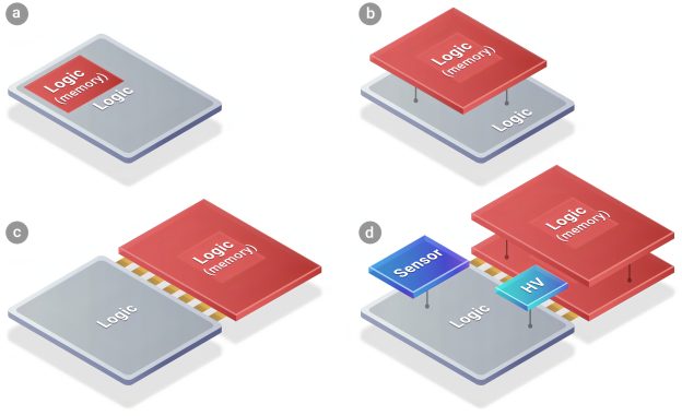
As outlined on TSMC’s website, SoIC technology integrates both homogeneous and heterogeneous chiplets into a single SoC-like device. With a smaller footprint and thinner profile, the chip can be seamlessly incorporated into advanced packaging platforms such as CoWoS and InFO. While it appears externally as a conventional SoC, it internally combines multiple functions through heterogeneous integration.
Currently, TSMC’s main SoIC capacity is located at AP6 in Zhunan, Miaoli, with additional support from AP5B in Taichung, as Commercial Times indicates.
Read more
- [News] TSMC Reportedly to Break Ground on U.S. Advanced Packaging Plants in 2028, Starting with SoIC
- [News] TSMC Advanced Packaging CapEx Projected to Grow 24% CAGR in 2025–27; AP7 Eyes WMCM, CoPoS
(Photo credit: TSMC)
Please note that this article cites information from Commercial Times, TechPowerUp, and TSMC.


