[News] SKC Reportedly Channels Over Half of ₩1T Capital Increase Into Absolics to Fast-Track Glass Substrates
As traditional materials approach their physical limits, glass substrates are coming to the forefront of next-generation chip packaging. According to Global Economic, SKC recently announced plans to allocate more than ₩600 billion—over half of its ₩1 trillion capital increase—to its glass substrate subsidiary, Absolics.
Building on this investment momentum, Absolics is sharpening its roadmap. As reported by The Elec, the company is adopting a dual-track strategy: an embedded solution aimed at high-performance AI data center applications, alongside a non-embedded route designed for faster commercialization. The objective is to enter the market swiftly while establishing technological leadership.
SKC stated, as cited by the report, that Absolics has achieved meaningful progress in product development with global big tech clients. The company added that it recently appointed Kang Ji-ho, previously with Intel and SK hynix, as CEO to further bolster its technological expertise, as The Elec notes.
Absolics has completed the world’s first dedicated glass substrate manufacturing facility in Georgia, U.S., and is aiming to secure orders from major fabless players such as NVIDIA, Global Economic adds.
Experts cited by Global Economic say glass substrates could improve power efficiency by over 40% and reduce chip thickness by more than 25%. As stacking technologies near their limits, substrate-level innovation may deliver severalfold gains in AI accelerator performance, prompting firms such as Google and Microsoft to factor glass adoption into hardware design from the outset, Global Economic notes.
Global Players Race to Commercialize Glass Substrates
Tech companies are accelerating efforts to develop glass substrates. According to Chosun Biz, Samsung Electro-Mechanics has set up a pilot line at its Sejong facility, plans to supply prototypes this year, and is targeting mass production after 2027. LG Innotek also intends to build a pilot line at its Gumi plant by year-end and begin prototype production within the year.
Beyond South Korea, global players are also making moves. According to Global Economic, Intel has invested more than $1 billion to speed up glass substrate mass production and is aiming for standardization by 2030. Commercial Times reports that TSMC has formed a dedicated FOPLP R&D team and production line, advancing a roadmap that integrates panel-level packaging with TGV and glass substrates.
Japan’s Dai Nippon Printing (DNP) is likewise expanding its push. According to EE Times Japan, the company began phased operations of its new TGV glass core substrate pilot line in December 2025. Chinese players are also entering the field. Calian Press reports that Apple supplier Lens Technology has recently announced its entry into TGV glass substrates.
Read more
- [News] Samsung Reportedly Shifts Glass Substrate Project to Business Unit, Eyes 2027 Ramp-Up
- [News] DNP Advances TGV Glass Substrates, Eyes Early-2026 Sample Shipments, FY2028 Mass Production
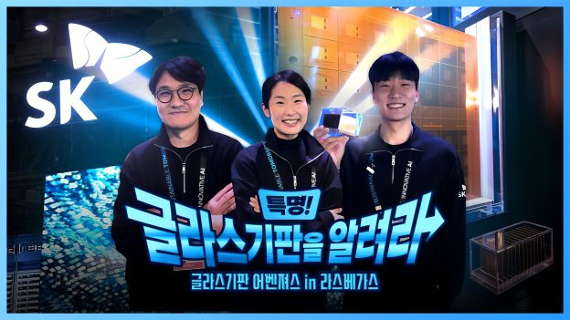
(Photo credit: SKC on LinkedIn)
Please note that this article cites information from Global Economic, The Elec, Chosun Biz, Commercial Times, EE Times Japan, and Calian Press.


