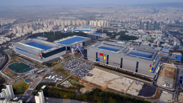
[News] Samsung Reportedly Ends Last 2D NAND Line as Early as March, Repurposes Facility for 1C DRAM
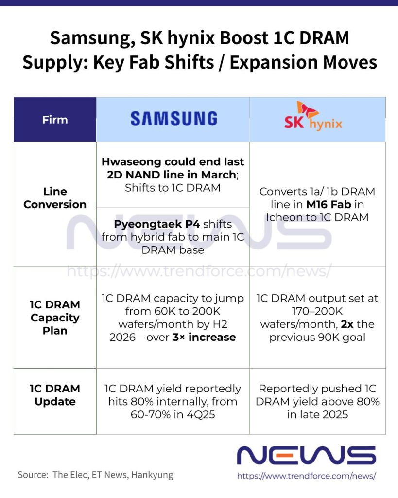
Amid tightening memory supply, cutting MLC NAND output is becoming a clear trend among major memory makers—but Samsung’s 2D NAND era could end sooner than expected. According to The Elec, the company may halt 2D NAND production at Hwaseong Line 12 as early as March and converting the facility into a 1C DRAM end fab to ease production bottlenecks.
The Elec says the line, with a monthly output of roughly 80,000–100,000 12-inch wafers, will pivot to late-stage DRAM processes, including wiring. Samsung informed customers of the planned shutdown as early as last year, the report adds.
According to The Elec, this move officially closes Samsung’s 2D NAND chapter. The company first mass-produced 1Gb NAND flash in 2002 and broke new ground in 2013 with mass production of 3D V-NAND. Now, roughly 13 years after the first 3D NAND rolled off the line, Samsung is shutting its last 2D NAND facility, the report notes.
Xi’an Plant Steps In as South Korea Cuts NAND Output
As highlighted by the report, the NAND volume reduced in South Korea is expected to be replaced by Samsung’s Xi’an plant in China, which is undergoing a transition of its 3D NAND lines to advanced-generation processes.
As previously reported by Global Economic, Samsung’s Xi’an plant, which now accounts for roughly 40% of the company’s total NAND output, is rapidly moving up the technology ladder as well— transitioning from 128‑layer (6th‑generation) products toward 200‑layer and beyond (8th‑generation V8) NAND processes.
Samsung, SK hynix Ramp up 1C DRAM Capacity
Samsung’s move fits its broader memory strategy, as 1C DRAM is not only the core of next-generation HBM4 but also expanding into general-purpose server products.
According to The Elec, the company is boosting 1C DRAM investments across Pyeongtaek and Hwaseong. Pyeongtaek’s P4 was originally designed as a hybrid fab for DRAM, NAND, and foundry production, but recent plans have reportedly shifted its focus entirely to DRAM. Older Hwaseong lines are also being upgraded to 1C DRAM processes, the report adds.
Samsung’s archrival SK hynix is accelerating its 1C DRAM investments as well. As per The Elec, SK hynix expects to churn out 170,000–200,000 wafers per month for 1C DRAM alone—up from the 90,000 wafers per month initially planned last April.
Meanwhile, SK hynix is also moving to upgrade its M16 fab, converting the 1a DRAM line to 1C DRAM by next year, The Elec notes, adding a 1b DRAM line is slated to follow suit within the same timeframe.
Against this backdrop, on Feb. 25, SK hynix said it will invest about 21.6 trillion KRW (USD 15 billion) in the first fab in the massive Yongin Semiconductor Cluster by December 2030, bringing total investment for the facility to roughly 31 trillion KRW (USD 21.5 billion).
Read more
- [News] NAND Giants Reportedly Cut Output in 2H25 as Prices Surge; Samsung Mulls 20–30% Hike in 2026
- [News] Samsung, Micron Rumored to Exit MLC, Driving Price Hikes and Order Surge for Taiwanese Suppliers
(Photo credit: Samsung)
Please note that this article cites information from The Elec, Global Economic and SK hynix.


