[News] Breaking HBM Barriers: Samsung’s zHBM vs. Intel’s Z-Angle Memory

As conventional HBM designs continue to face thermal and stacking limits, major semiconductor players are exploring innovative memory architectures. In early February, Intel, in collaboration with SoftBank’s subsidiary SAIMEMORY, showcased a prototype of Z-Angle Memory (ZAM). Meanwhile, ZDNet reports that Samsung revealed the detailed specifications of ‘zHBM’, a next-generation architecture succeeding HBM4, at SEMICON Korea 2026—marking its first public disclosure.
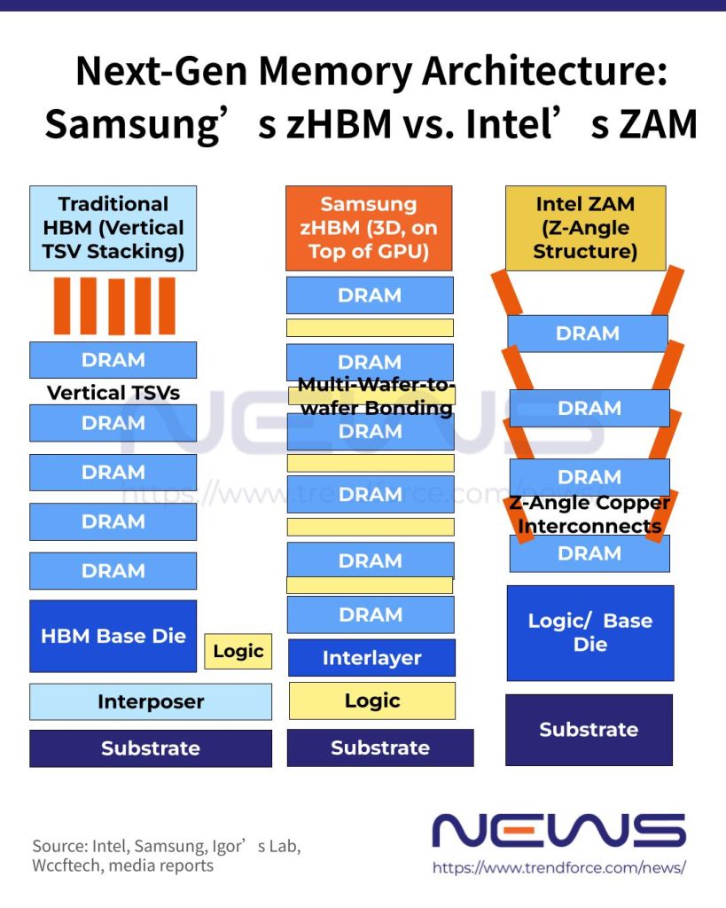
Both solutions embrace the “z-axis” concept, but how do their approaches differ? Here’s a quick breakdown comparing the new architectures from the two chip giants with traditional DRAM stacking.
Traditional Approach
As explained by the Chosun Daily, HBM stacks DRAM dies like a tall building, connecting them vertically through through-silicon vias (TSVs)—essentially tiny silicon “elevators” that move data between layers. According to Cadence’s definition, a TSV is essentially a vertical metal pillar—usually made of copper—that passes through the entire thickness of a silicon die.
The Chosun Daily further notes that a single HBM can contain over 10,000 TSVs, enabling very short data paths and high speed. However, this vertical design also traps heat in the center, making thermal dissipation challenging, the report adds.
Samsung’s Approach: Next Leap in 3D Memory Technology
To further improve performance and efficiency, Samsung comes up with zHBM, the futuristic memory architecture coming after 6th-gen HBM4. According to the Herald Business, unlike current HBM, which sits beside the GPU, Samsung aims to evolve this into a fully 3D structure with HBM stacked directly on top of the GPU, promising tighter integration and improved performance.
Jaehyuk Song, CTO of Samsung Electronics’ Device Solutions Division, told the report that early tests show the solution could achieve up to four times the bandwidth and energy efficiency of HBM4.
ZDNet further points out that zHBM leverages multi-wafer-to-wafer bonding technology, enabling tens of thousands of I/O terminals. In addition to the bandwidth boost, this approach aims to reduce power consumption by 75% as well, the report adds.
Intel’s ZAM: Diagonal Stacking Tackles Heat and Power
Samsung’s approach promises a huge boost in HBM bandwidth, though it doesn’t directly tackle the thermal bottleneck—a challenge Intel seems to be focusing on instead.
As reported by PC Watch, traditional memory has been built using a planar stacking structure, but this design is hitting its limits—current implementations already push 16 layers close to the maximum, with most estimates putting the upper bound at around 20 layers due to power and thermal constraints.
On the other hand, Igor’s Lab explains that at the core of ZAM architecture is a diagonal interconnect. Unlike HBM, which uses vertical TSVs, ZAM routes connections diagonally through the stack.
As noted by Igor’s Lab, TSVs create hotspots and mechanical stress, which worsen as bandwidth rises. ZAM’s diagonal copper paths, in contrast, improve heat flow and boost energy efficiency. Intel claims this could cut power consumption by 40–50%, a bold move that, if realized, would challenge HBM’s efficiency, which still depends heavily on packaging and interposer design, the report adds.
Even more striking is the reported 512 GB capacity per chip, far surpassing current HBM stacks, Igor’s Lab notes.
Uncertain Future
However, both chipmakers are still a few years away from seeing these technologies in production, and real-world performance remains untested, making it too early to draw firm conclusions.
Intel has said that ZAM prototypes are expected in 2027, with a full-scale rollout targeted for 2030. Samsung, meanwhile, has not disclosed a concrete timeline for zHBM, but highlighted Hybrid Copper Bonding (HCB) for next-generation HBM development.
According to News 1, Samsung says applying HCB to 12- and 16-layer stacks could reduce thermal resistance by over 20% and lower base die temperature by more than 12% compared with conventional thermal compression bonding. The company has not yet announced when HCB will be applied to actual HBM production, the report adds.
In short, the true impact on HBM performance and AI workloads will only be clear once prototypes and production units are tested. Still, these different DRAM stacking approaches open up new possibilities for overcoming current thermal and layer-density limits.
Read more
- [News] First Look at ZAM: SAIMEMORY Unveils Memory to Address Thermal Issues at Intel’s Japan Event
- [News] Intel Reenters DRAM Race? A Closer Look at the Z-Angle Memory Collaboration with SoftBank
(Photo credit: Intel Japan’s X)
Please note that this article cites information from ZDNet, Chosun Daily, Cadence, Herald Business, PC Watch, Igor’s Lab and News 1.


