[News] TSMC Reportedly Suspends New 3nm Kick-offs, Steers Customers to 2nm to Optimize Costs
TSMC recently announced the successful mass production of its 2nm process, while industry rumors suggest the company has put new 3nm projects on hold. According to Commercial Times, sources indicate that TSMC has not only raised prices for its 3nm process this year, but has also temporarily suspended kick-offs for new 3nm projects. The report notes that this is mainly due to fully booked orders, with short-term capacity expansion unable to keep pace with the influx of customer demand.
Although TSMC’s 3nm family spans multiple variants, current capacity has been completely absorbed by customers including AI GPUs, cloud data center ASICs, and high-end mobile application processors, the report adds.
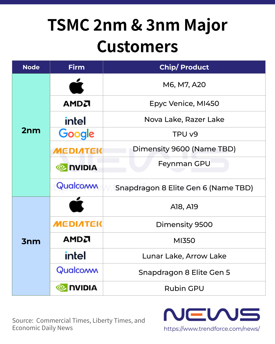
From a strategic perspective, TSMC is also seeking to guide customers to shift new product planning earlier toward its 2nm node, which offers a more favorable cost structure. With the 2nm process now entering mass production, major customers are said to include mobile chipmakers such as Apple, Qualcomm, and MediaTek.
Notably, industry sources cited in the report indicate that 2nm pricing is not as high as market speculation suggesting wafers priced above US$30,000. Even so, compared with N3P, prices have seen a meaningful increase. That said, by leveraging chiplet-based die configurations and spreading costs across large shipment volumes, SoCs—unlike memory chips—are not the primary driver behind sharp increases in smartphone bills of materials (BOM), the report adds.
TSMC’s 2nm Transition: Technology, Costs, and Strategy
The 2nm node marks a key inflection point in TSMC’s advanced-process roadmap. It introduces the nanosheet transistor architecture, delivering clear gains in performance, power efficiency, and transistor density, while also offering a more favorable cost structure at the process design level. The report notes that, compared with 3nm, the adoption of advanced techniques such as atomic layer deposition (ALD) has not resulted in a significant increase in the number of EUV exposure layers, helping keep per-die manufacturing costs competitive and reinforcing TSMC’s push to transition customers to the 2nm node.
Industry sources cited by the report add that the shift to a GAAFET-based process moves wafer fabrication from planar patterning to true three-dimensional construction, sharply increasing process complexity and elevating the importance of materials technologies. In particular, ALD must deposit uniform, defect-free dielectric layers and metal gates around suspended structures, placing exceptionally high demands on deposition uniformity and process control.
Read more
- [News] Earnings Call Preview: TSMC 2nm in Focus — Capacity, Sales Contribution, and More
- [News] TSMC Reportedly to Raise Sub-3nm Prices 3-10% in 2026, Plans Hikes Through 2029
(Photo credit: TSMC)
Please note that this article cites information from Commercial Times.


