Popular Keywords


3nm
News

[News] TSMC N3 Tightens on AI Demand; Arizona 2nd Fab 3nm Volume Production in 2H27, Kumamoto in 2028
TSMC holds its earnings call today, with tightness at its 3nm node coming into focus as the foundry giant outlines new plans to expand N3 capacity. Its Chairman and CEO C.C. Wei says that, historically, TSMC does not add capacity once a node reaches its target level; however, in response to strong A...
News
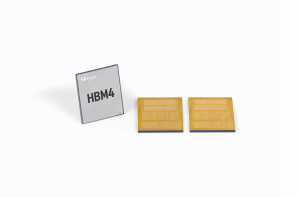
[News] SK hynix Reportedly Weighs TSMC 3nm for HBM4E Logic Dies to Gain Edge over Samsung
Please note that this article cites information from the Chosun Daily, ETNews, and TechPowerUp. With all three leading memory giants now close to shipping HBM4, the race for next-gen HBM is intensifying, with advanced nodes taking center stage. Samsung is reportedly set to use its in-house 4nm pr...
News
[News] TSMC’s Kumamoto 3nm Upgrade Highlights Overseas Output Reportedly Hitting 20% by 2028
TSMC’s surprise move to upgrade Kumamoto Fab 2 to 3nm—lifting total investment to about US$17 billion—has put its overseas footprint back in the spotlight. Citing analysts, Economic Daily News reports that as U.S., Japan, and Germany fabs ramp, overseas capacity is set to reach ~20% or more of...
News
[News] TSMC Earnings Preview: $150B Capex Over Next Three Years Tops Five Key Focuses
Ahead of TSMC’s earnings call on January 15, the market has already been flooded with reports that the company may build five additional fabs in Arizona under a U.S.–Taiwan trade framework. But what else should investors be watching when results are released tomorrow? A TechNews report flags ...
News

[News] TSMC Reportedly Suspends New 3nm Kick-offs, Steers Customers to 2nm to Optimize Costs
TSMC recently announced the successful mass production of its 2nm process, while industry rumors suggest the company has put new 3nm projects on hold. According to Commercial Times, sources indicate that TSMC has not only raised prices for its 3nm process this year, but has also temporarily suspend...
- Page 1
- 13 page(s)
- 62 result(s)