[News] Arizona Rises as U.S. Chip Hub: SEMICON West Highlights TSMC, Intel, and Growing Semiconductor Cluster
With semiconductor heavyweights led by TSMC and Intel ramping up U.S. manufacturing, Arizona has emerged as a powerhouse for advanced chipmaking. As Commercial Times notes, SEMICON West—scheduled for October 7‑9, 2025—marks the first time the event moves from San Francisco to Phoenix, highlighting the region’s growing prominence.
As noted by the report, the relocation signals the rise of the U.S. Southwest as a key semiconductor hub, where front-end wafer fabrication, back-end advanced packaging, talent development, and R&D platforms are taking shape.
Notably, a couple of days ago, Intel also kicked off its first Intel Tech Tour in Arizona, and is unveiling details on its first in-house 18A processor, Panther Lake, on October 9, according to TweakTown. As Commercial Times reported, with Intel’s 18A starting production in Arizona, the site will become the first in the U.S. to enter 2nm-class mass production.
TSMC, Intel Ramp up in South West
As Economic Daily News previously reported, TSMC, with its $165 billion U.S. investment, is moving faster in Arizona. Its third fab could enter mass production as early as 2027—beating the original schedule by a full year. Moreover, the report highlights that this facility is poised to host TSMC’s most advanced nodes, including 2nm and angstrom-class A16 processes, which had initially been slated for 2028.
On the other hand, Commercial Times notes that beyond TSMC, Intel is building Fab 52 and Fab 62 in Chandler, and could expand advanced fabrication and packaging investments across Arizona, New Mexico, Ohio, and Oregon. These moves are fostering a cluster effect, boosting the influence of domestic IDM fabs and solidifying the Phoenix-area semiconductor ecosystem, the report adds.
As Commercial Times explains, Intel’s Fab 52 alone is expected to reach 1,000–5,000 wafers per month by year-end, ramp to 15,000 in 2026, and ultimately hit 30,000.
Advanced Packaging Momentum Brewing
Additionally, advanced packaging hubs are taking shape on the site. Amkor, according to its press release, has begun building a new advanced semiconductor packaging and testing campus in Arizona, increasing its planned investment from USD 2 billion to USD 7 billion.
Once finished, the campus will boast over 750,000 sq ft of cleanroom space and accommodate up to 3,000 employees, the company said. The first phase is slated for mid-2027 completion, with full-scale production kicking off in early 2028.
Commercial Times notes that a growing talent and R&D ecosystem is also taking shape, highlighting Arizona State University (ASU) for its large-scale cleanrooms and production-grade lab facilities. In early 2025, the U.S. Department of Commerce announced a new CHIPS R&D hub at ASU, focused on 300 mm fabrication and advanced packaging research, which is expected to be operational by 2028, the report adds.
Thus, the report notes that hosting SEMICON West in Phoenix carries symbolic significance: with front-end manufacturing, advanced packaging, and talent pipelines all ramping up simultaneously, system integrators and Taiwanese suppliers can adopt a “service first, manufacturing later” approach, gradually localizing modules and key components as demand grows.
Read more
- [News] TSMC Reportedly Pulls Arizona Third Fab to 2027, Ahead by One Year, Eyeing 2nm and A16
- [News] Intel to Unveil 18A at Tech Tour: Reportedly Limited Q3 Shipments, Panther Lake Debuts Oct. 9
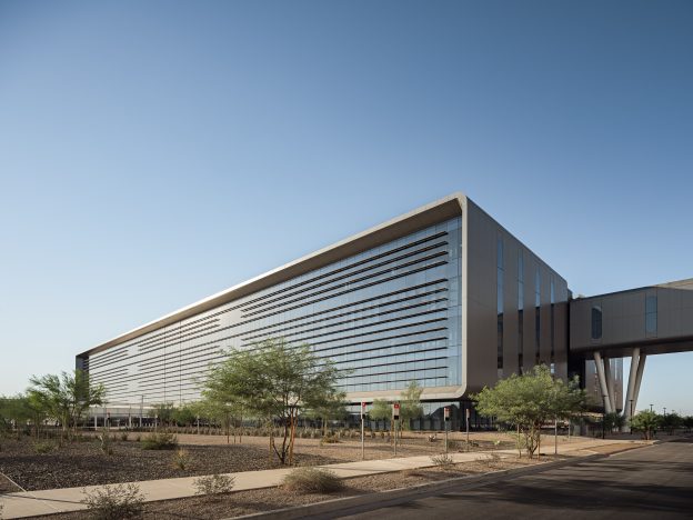
(Photo credit: TSMC)
Please note that this article cites information from Commercial Times, TweakTown, Amkor and Economic Daily News.


