[News] TSMC Reportedly Delays Kumamoto 2nd Fab Launch to 2029 Amid U.S. Expansion Push
TSMC’s U.S. expansion has been accelerating, but its plans in Japan are reportedly facing renewed delays. According to MoneyDJ, citing Nikkan Kogyo Shimbun, the launch of TSMC’s second fab in Kumamoto could be postponed by up to a year and a half, with operations now expected to begin in the first half of 2029.
TSMC’s second Kumamoto fab was originally scheduled to begin construction in Q1 2025, but the timeline was later pushed back to “sometime in 2025.” As The Wall Street Journal notes, TSMC Chairman and CEO C.C. Wei stated in June that the delay was due to traffic-related issues, the report notes.
However, as highlighted by The Wall Street Journal on the 4th, citing sources, further delays to the project are likely, as the company prioritizes investments in its U.S. facilities in response to tariff policies under the Trump administration. The report adds that the start of construction can no longer be forecast with certainty.
In addition, Economic Daily News notes that the delay in TSMC’s second Kumamoto fab may stem from weaker-than-expected demand from key customers. The report states that the fab adopted 7nm and 6nm processes to support Sony and Denso’s production of microcontrollers and sensors, but few Japanese clients currently require such advanced technologies.
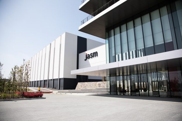
As indicated by MoneyDJ, TSMC Chairman and CEO C.C. Wei stated during the company’s Q2 earnings call that, with strong support from central and local governments in Japan, the first specialty process wafer fab in Kumamoto began volume production in the second half of 2024 and is achieving good yield performance.
MoneyDJ states that the first Kumamoto fab produces 12nm to 28nm logic chips, while the second is planned to manufacture Japan’s most advanced 6nm products. Based on 12-inch wafer equivalents, the combined monthly capacity of both fabs is expected to exceed 100,000 wafers. Total investment in the two facilities is projected at approximately JPY 2.96 trillion, with the Japanese government providing up to JPY 1.2 trillion in subsidies, as MoneyDJ points out.
Read more
- [News] TSMC Accelerates 2nd Arizona Fab Production; Ramp-Up Schedules for Japan, Germany Undisclosed
- [News] TSMC Chair Reportedly Confirms 2nd Kumamoto Fab Construction Delayed to Mid-2025 Due to Traffic
(Photo credit: TSMC)
Please note that this article cites information from MoneyDJ, Nikkan Kogyo Shimbun, The Wall Street Journal, and Economic Daily News.


