[News] Nikon Unveils DSP-100 System for Panel-Level Packaging, Supporting 600mm Panels with 9x Throughput
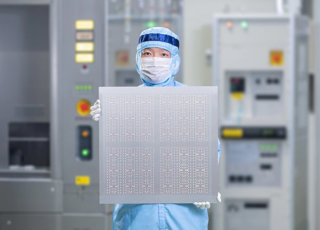
As semiconductor giants embrace fan-out panel-level packaging (FOPLP) for larger, more efficient chip designs, Japan’s Nikon is joining the race. The company has begun taking orders in July for its new DSP-100 digital lithography system, designed specifically for 600 mm square panels used in advanced AI chip packaging, according to its press release and reports from TechPowerUp and XenoSpectrum.
Nikon expects to ship the first DSP-100 units in fiscal 2026. As noted by TechPowerUp, the system supports an industry-wide shift—led by TSMC, Intel, and Samsung—away from the limitations of 300 mm wafers. Economic Daily News previously revealed that TSMC aims to launch pilot production of its FOPLP technology in 2027, starting with a 300×300 mm panel—smaller than the 510×515 mm format used in earlier tests.
While TSMC may initially skip the larger 510×515 mm format, Nikon goes even further—its new system supports exposure on 600×600 mm glass or resin panels, unlocking greater packaging potential, as noted by TechPowerUp.
Nikon says the DSP-100 achieves 1.0 µm line-and-space resolution, ±0.3 µm overlay accuracy, and processes up to 50 panels per hour at 510×515 mm. Moreover, it supports exposure on panels as large as 600×600 mm—enabling up to 9× higher productivity per substrate for 100 mm chip packages compared to 300 mm wafers.
Additionally, the system offers high-precision correction for substrate warpage and deformation, reducing production costs with maskless technology and minimizing maintenance costs with solid state light sources, Nikon says.
Samsung’s Progress
On the other hand, Samsung currently offers advanced packaging solutions like I-Cube 2.5D, X-Cube 3D IC, and 2D IC packaging. For low-power memory integration in devices such as mobiles and wearables, it provides fan-out panel-level and wafer-level packaging platforms. According to Newsis, Samsung has applied PLP to chips like the Exynos W920 in Galaxy Watch and reportedly to Google’s Tensor G4 for Pixel phones.
However, Samsung’s use of PLP is still mostly confined to mobile chips and power management ICs. Industry experts warn that to stay competitive, Samsung must expand PLP technology into AI and high-performance computing (HPC) applications, the report notes.
Read more
- [News] FOPLP Heats Up: ASE, Powertech Expand; TSMC Reportedly Preps 2026 CoPoS Pilot Line
- [News] TSMC Reportedly Gears Up for CoPoS Mass Production by 2029, Tapping NVIDIA as First Client
- [News] Wafer-Level Packaging Showdown: TSMC Scales up CoWoS Reticle Size, as Intel Readies Foveros-S
(Photo credit: Nikon)
Please note that this article cites information from TechPowerUp, XenoSpectrum, Economic Daily News, Newsis, and Nikon.


