


[News] Samsung Reportedly Eyes In-House Silicon Photonics PIC Testing by End-2026 with TSMC-Qualified Tools
Samsung is stepping up its silicon photonics development by bringing key testing capabilities in-house. According to The Elec, sources say Samsung is testing silicon photonics photonic integrated circuit (PIC) wafers using probe stations from U.S.-based FormFactor and Taiwan-based MPI, with plans to complete in-house PIC wafer testing by the end of 2026.
Notably, FormFactor and MPI are so far the only two probe station suppliers to have passed TSMC’s equipment qualification for CPO-related testing, according to the report. TSMC uses their equipment to develop and validate its Compact Universal Photonic Engine (COUPE), its silicon photonics-based co-packaged optics (CPO) platform. TSMC said a true co-packaged optics solution using COUPE on substrate is set to begin production in 2026.
Samsung had outsourced PIC wafer validation to external organizations, including Belgian semiconductor research institute imec, since last year. It has since established its own testing environment and is conducting repeated evaluations. The company is now optimizing its initial PIC designs by measuring wafer performance and feeding the results back into the design process. Samsung is also preparing for customer evaluations, with global networking and communications chipmakers including Broadcom cited as potential customers, according to the report.
Silicon photonics probe stations connect PIC wafers to optical and electrical measurement equipment while precisely aligning optical fibers with the chips’ optical input and output ports. This allows engineers to verify whether devices transmit light as designed and properly convert between electrical and optical signals while repeatedly testing individual dies across the wafer, the report adds.
As CPO moves from the lab toward commercialization, TrendForce notes that testing remains a major bottleneck to mass production, as the industry still lacks unified standards and many processes remain largely manual.
From PIC Testing to Optical Engines
After PIC testing, Samsung plans to move on to optical engines that integrate a PIC with an electronic integrated circuit (EIC), the report notes. While the PIC handles optical signals, the EIC processes and amplifies electrical signals to drive the PIC’s optical devices. The two are stacked together and connected to external optical fibers to form an optical engine. Samsung began developing EIC-PIC optical engines in 2026 and plans to start testing them in 2027, the report notes.
The efforts are part of Samsung’s broader silicon photonics roadmap. The Elec adds that Samsung plans to launch silicon photonics foundry services in 2027, offering optical device process and process design kits (PDKs) for customers to design PICs that Samsung Foundry will manufacture in wafer form. Samsung has also made early commercial progress: according to Maeil Business Newspaper, its foundry business has secured an order from a major optical communications module maker, laying the foundation for its silicon photonics business, with mass production for the project set to begin in the second half of 2026.
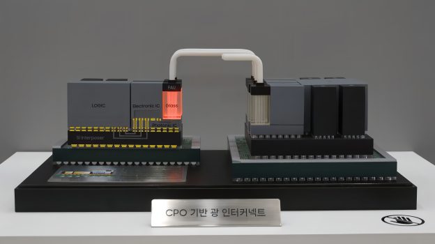
The longer-term goal is to integrate optical engines with logic chips and HBM, The Elec highlights. Samsung recently showcased a CPO mockup integrating an optical engine into a single package, demonstrating the integration of its silicon photonics foundry process with advanced packaging. The Elec adds that Samsung ultimately plans to expand CPO applications beyond network switches to GPUs and CPUs.
Samsung’s broader push comes as the CPO industry moves toward greater integration. TrendForce believes vertical integration is becoming the default playbook, and vendors that can control silicon photonics design, optical engine manufacturing, and advanced packaging in-house will be best positioned to lead once the CPO switch market hits its volume ramp in 2027–2028.
Read more
- CPO Testing: The Last Mile to Mass Production
- NVIDIA and Broadcom Begin Volume Ramp of CPO Switches, with Optical Engine Yield and Advanced Packaging Capacity Emerging as Key Expansion Bottlenecks, Says TrendForce
(Photo credit: Samsung)


