


[News] TSMC: SoIC, CoWoS to Drive 50× Compute by 2029; Silicon Photonics to Top 50% of Transceiver Market by 2027
TSMC is stepping up its technology roadmap to meet surging AI computing demand. According to TechNews, April Li, Global Head of AI and HPC Business Development at TSMC, said at SEMICON Taiwan 2026 that AI computing demand is growing fivefold annually, putting increasing pressure on compute capacity. In response, TSMC is integrating advanced process, 3DFabric, and silicon photonics into its HPC platform. Notably, the company expects SoIC and CoWoS integration to boost overall system computing performance to 50 times its 2024 level by 2029.
As the report indicates, Li said heterogeneous integration is the only way to push beyond current computing limits. TSMC plans N2P-on-N3P 3D integration in 2026, followed by A14-on-A14 in 2029, with interconnect pitch shrinking to 4.5 microns.
TSMC Advances COUPE and Silicon Photonics Design
TSMC is also continuing to advance its COUPE technology. According to TechNews, its 2–4-micron bonding pitch limits transmission loss at 112 Gbps to just 0.06 dB, compared with 1.38 dB for micro-bumps, helping reduce power consumption and latency to 10–20 nanoseconds.
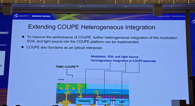
As Mirror Daily indicates, TSMC’s self-developed COUPE platform uses TSMC-SoIC bonding technology to integrate electronic integrated circuits (EICs) with photonic integrated circuits (PICs), while supporting both grating couplers (GCs) and edge couplers (ECs). To further scale bandwidth, TSMC is pursuing two development paths. One will increase per-channel speeds from 200 Gbps to more than 400 Gbps while expanding channel counts from 16 to over 128, lifting total bandwidth from 3.2 Tbps to more than 12.8 Tbps. The other will expand wavelength-division multiplexing (WDM) from a single wavelength to 4, 8, 16, and beyond.
The company is also addressing testing and design challenges as CPO moves toward broader deployment. According to Mirror Daily, TSMC has enabled wafer-level optical testing for edge-coupled devices, allowing defective dies to be screened out before costly CPO assembly. TechNews adds that TSMC has introduced an optical PDK that enables electronic-photonic co-simulation to address key silicon photonics design challenges, while Mirror Media notes that the PDK supports Cadence and Synopsys tools to help accelerate product development.
Silicon Photonics Gains Ground as CPO Nears Mass Production
Beyond TSMC’s technology roadmap, silicon photonics is moving toward broader adoption and large-scale CPO deployment. As noted by Central News Agency, TSMC Vice President of Advanced Packaging Technology and Service K.C. Hsu said optical transceiver architectures are undergoing a structural shift, with silicon photonics expected to account for more than 50% of the optical transceiver market by 2027. CPO represents the next step, with some suppliers expected to begin mass production in the second half of 2026.
Hsu described optics as the “nervous system” of data centers as demand for high-speed connectivity grows. As noted by Central News Agency, he said optical transceiver sales rose 25% in 2025 and are expected to grow another 50% in 2026, while the high-end 100G-and-above market doubled in 2024 and expanded another 60% in 2025.
Hsu noted that Taiwan’s silicon foundry ecosystem is already capable of producing optical engines at scale and with high precision, while real-world data and market validation are helping ease longstanding concerns over CPO reliability. The bigger challenge to large-scale deployment now lies elsewhere in the supply chain, including lasers, optical fibers, fiber connectors, and product testing, he said, as reported by Central News Agency.
Read more
- [News] TSMC PIC Capacity Seen Surging to 25K Wafers/Month by 2028; NVIDIA, Broadcom Eyed as Early COUPE Customers
- [News] TSMC Targets 2H26 COUPE on Substrate; NVIDIA Could Eye Long-Term Substrate Deals Amid CPO Push
(Photo credit: TrendForce)


