


[News] Shinko Electric Advances 22-Layer Glass Substrates; Samsung Electronic Mechanics Faces Ramp-Up Uncertainty
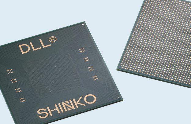
The glass substrate race is heating up as AI chips demand larger packages, with South Korean and Japanese players racing to gain an early edge. According to Seoul Economic Daily, Japan’s Shinko Electric Industries has developed a 22-layer glass substrate by stacking 11 copper wiring layers on each side, addressing the so-called “SeWaRe” issue of internal cracking or delamination.
As explained by the report, the shift toward larger AI packages is exposing the warpage limits of conventional organic substrates. By contrast, glass offers greater rigidity and less thermal deformation, making it a stronger fit for large, high-performance AI chips.
Shinko Electric showcased its latest glass-core substrate at the Advanced Packaging Summit 2026 in July. According to SEMI, Shinko Electric reinforced the substrate’s edges with resin to disperse stress and suppress SeWaRe defects under thermal loading. The company also applied an edge-protection material to disperse stress concentrated at the substrate edges, helping suppress SeWaRe defects under thermal loading.
The result, as noted by the company, is a 22-layer glass-core build-up substrate, featuring 11 copper wiring layers on each side.
Notably, Japanese players appear to have the technological edge so far compared with its South Korean peers, Seoul Economic Daily reports. Among them, Shinko Electric has developed through-glass via (TGV) technology for forming microscopic vertical holes through glass, as well as multilayer insulation and copper wiring processes, the report notes, adding that Japan’s DNP launched a TGV glass substrate pilot line in Saitama last December, targeting mass production in 2028.
Samsung Electronic Mechanics Races to Close the Gap Amid Mass-Production Uncertainty
Meanwhile, Seoul Economic Daily highlights Samsung Electro-Mechanics’ efforts to catch up with Japanese rivals. The company, per the report, is accelerating its glass substrate push through GlaSSEM, a JV with Dongwoo Fine-Chem, the Korean subsidiary of Japan’s Sumitomo Chemical.
The report further explains that Samsung Electro-Mechanics’ push into glass substrates is closely tied to FC-BGA package substrates for AI semiconductors, while growing package sizes are driving Big Tech demand for glass substrates that can minimize warpage even in large-area applications. According to the report, product validation with customers is already underway.
However, the ramp-up timeline remains uncertain. The Elec reports that GlaSSEM has yet to provide equipment suppliers with a firm ordering schedule. Samsung Electro-Mechanics first notified suppliers of planned orders in November 2025, but the timeline has reportedly since been pushed back at least three times, from December to March and then June.
The delays may be linked to a failed reliability qualification for glass substrate prototypes at a global communications chip customer, industry sources told The Elec. With new prototypes now requiring development and resubmission, production-line construction may not begin until 2H27, potentially pushing mass production to 2028 or later, the report adds.
On August 19, Samsung Electro-Mechanics stated that there has been no failed customer qualification, and customer evaluation is currently ongoing. The target timeline remains 2H27 for glass core material and 2028 for finished glass substrates.
Read more
- [News] SKC Reportedly Pushes Glass Substrate Mass Production to 2027, Targets Final Validation by Year-end
- [News] Glass Substrates Eye 2027 Launch, Scale Toward 2030 as CoWoS Costs Rise and Hyperscaler Demand Grows
(Photo credit: Shinko Electric)


