


[News] TSMC Reportedly Eyes Two AUO Fabs Worth TWD 30B+ for FOPLP and CoPoS; Longtan Could Add 1.4nm
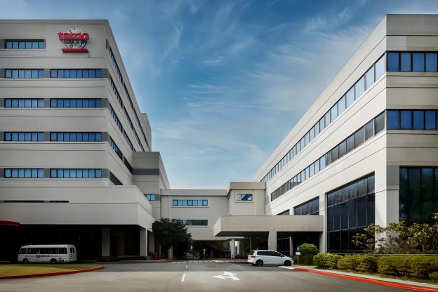
TSMC is reportedly looking to accelerate its advanced packaging expansion by securing existing manufacturing infrastructure near its key production hubs. According to Economic Daily News, sources say TSMC plans to acquire AUO’s L7 and L5C fabs near its Central Taiwan Science Park facilities to expand advanced packaging capacity. The two fabs are reportedly under negotiation, though no agreement has been signed or officially announced. The reported transaction is estimated to exceed TWD 30 billion, which would make it the largest sale of older-generation fabs by a Taiwanese panel maker in recent years.
As the report indicates, advanced packaging is moving toward a shift “from round to square,” with traditional round silicon wafers giving way to panel-format glass substrates and other materials. Following a model similar to Innolux’s, TSMC and AUO may collaborate on fan-out panel-level packaging (FOPLP) and Chip-on-Panel-on-Substrate (CoPoS), leveraging AUO’s strengths in glass substrates to establish an integrated manufacturing base spanning advanced processes and advanced packaging.
AUO’s Central Taiwan Science Park facility is located adjacent to TSMC’s Fab 15 complex. According to Economic Daily News, Fab 15A, which primarily focuses on mature 28nm to 22nm nodes, is planned to be upgraded to 4nm, while Fab 15B mainly produces chips using the 7nm node.
As noted by another report from Economic Daily News, TSMC Chairman and CEO C.C. Wei said its CoPoS pilot line is under construction, with technology and yields expected to take about another year to mature before customer production. The report highlights that TSMC could initially use 310mm × 310mm panels, with equipment and material validation in 2026, small-volume trial production in 2027, and mass production expected as early as 2H28–2029.
As TSMC, ASE, and others ramp advanced packaging capacity, older-generation panel fabs with large cleanrooms and ample power supply are becoming increasingly sought after. The report notes that repurposing these facilities for semiconductor glass substrates could help panel makers enter the higher-margin AI advanced packaging supply chain.
Notably, another Economic Daily News report says AUO plans to jointly develop glass substrate technologies with partners. Its board recently approved TWD 8.64 billion in capital expenditures, including pilot lines for through-glass vias (TGV), redistribution layers (RDL), and glass cores.
TSMC Eyes Longtan Expansion for 1.4nm and Panel-Level Packaging
Beyond acquiring existing facilities, TSMC is also exploring new sites to support its next wave of advanced manufacturing and packaging capacity. According to Liberty Times, the long-delayed third-phase expansion of the Longtan Science Park has resumed, covering about 104 hectares and providing roughly 46 hectares of industrial land. Sources say that once the expansion is completed, TSMC could build two 1.4nm fabs and one panel-level packaging facility at the site, though the final plans are still under consideration.
Read more
- [News] TSMC Reportedly Runs Dual-Track Evaluation on CoPoS Pilot Line, Sparking Global, Local Vendor Competition
- [News] TSMC Reportedly Expands Outsourcing of Key CoWoS Front-End Step to OSATs Amid Rising NVIDIA, ASIC Demand
(Photo credit: TSMC)


