[News] 18 Chinese Enterprises Accelerate Positions in Glass Core Substrate Market
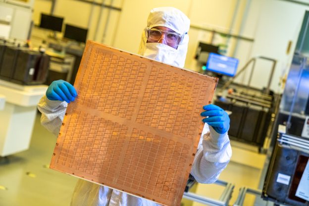
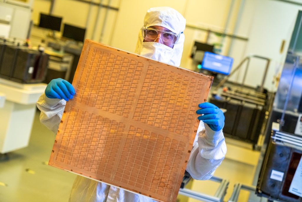
Global tech giants are accelerating their investments in glass-based advanced packaging. Intel recently entered a strategic partnership with Lens Technology to address bottlenecks of advanced packaging using TGV (Through Glass Via) technology, while BOE announced its full-scale entry into the AI semiconductor glass substrate market.
Earlier, Samsung Display reportedly established a dedicated TGV interposer R&D team, and Intel CEO Lip-Bu Tan publicly highlighted the company’s investment in 3D Glass Solutions (3DGS) engaging in glass substrate market.
Several months ago, Corning introduced its “Glass Bridge” architecture incorporating TGV for Co-Packaged Optics (CPO) next-generation designs, building a glass-based optical interconnect ecosystem tailored for AI data centers.
These synchronized moves point to a unified structural trend: as AI compute chips demand higher interconnect speeds, tighter packaging density, and superior thermal dissipation, conventional organic substrates and silicon interposers are reaching physical limitations. Featuring a low coefficient of thermal expansion (CTE), high dimensional stability, low dielectric loss, and compatibility with large-panel processing, glass has emerged as a premier candidate material for next-generation advanced packaging.
Industry Chain Takes Shape: From Raw Materials to Advanced Packaging
The glass core substrate value chain is structured into three distinct tiers:
- Upstream: Specialty raw glass sheets, along with core equipment and materials including ultrafast lasers, wet etching tools, physical vapor deposition (PVD), and electroplating systems.
- Midstream (Highest Value Share): High-precision processes including glass thinning, TGV micro-hole drilling, metallization/copper filling, chemical mechanical planarization (CMP), and Redistribution Layer (RDL) fabrication to produce Glass Interposers or Glass Core Substrates.
- Downstream: Advanced packaging for AI computing chips. Driven by Chiplets, High Bandwidth Memory (HBM), and CPO, glass substrates are evolving from conventional electrical interconnects into dual-function optoelectronic carriers.
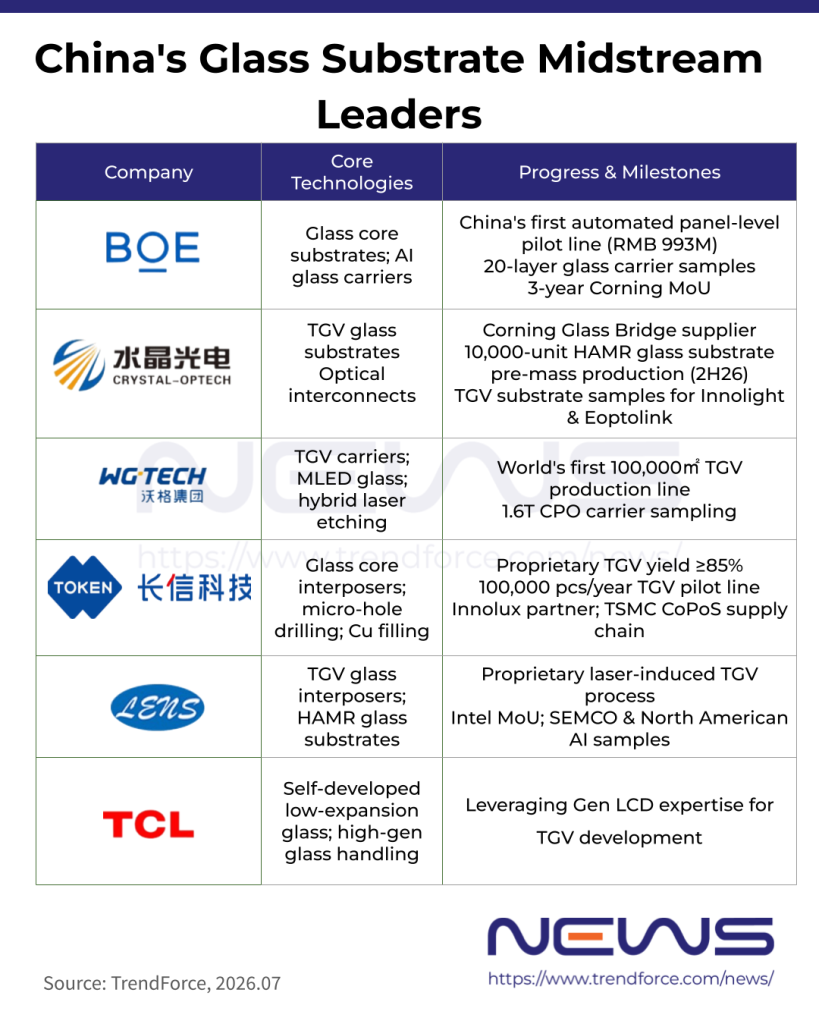
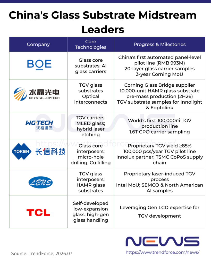
Chinese glass core substrate industry landscape: 18 listed companies’ current developments:
Within the midstream tier, Crystal-Optech, WG Tech, and BOE possess end-to-end manufacturing capabilities and have progressed into pilot/mass production lines and tier-1 vendor validation stages.
Key Midstream Players:
Crystal-Optech: Deeply integrated into Corning’s optical communication ecosystem. In the Heat-Assisted Magnetic Recording (HAMR) storage segment, the company has completed process integration across raw glass sourcing, ultra-thin processing, and precision drilling. It operates two primary growth vectors:
- HAMR Glass Platter Substrates: Pre-mass production small-batch shipments scheduled for H2 2026.
- Proprietary TGV Optical Interconnect Substrates: Designed for 1.6T/3.2T high-speed CPO modules, currently undergoing joint R&D validation.
Additionally, Crystal-Optech serves as the exclusive domestic optical path supplier for Corning’s Glass Bridge, with microlens and coupling coating samples slated for customer verification in H2 2026.
WG Tech: Leading domestic TGV process development through its subsidiary, TGV Circuits. Utilizing self-developed ultrafast laser hybrid etching, the firm achieves minimum hole diameters of ≤5μm and aspect ratios up to 100:1.
Its Wuhan facility houses the world’s first glass-based TGV multilayer circuit board production line with a planned annual capacity of 100,000㎡, and is currently delivering small-batch samples of 1.6T CPO carrier boards. Although revenue contribution remains modest prior to full scale-up, its integrated manufacturing capability ranks among global leaders.
BOE: BOE has fully automated its CNY 993 million glass-based packaging substrate pilot line, mastering high-precision TGV drilling and void-free deep-hole copper filling. Prototypes of 20-layer large-format glass carriers for compute chips have been delivered to leading AI chip vendors. In May 2026, BOE signed a three-year MoU with Corning to establish a joint task force on Micro LED optical interconnects and glass-substrate CPO technology.
TCL CSOT & Tianma Microelectronics: Both display makers are exploring TGV glass technology in early R&D phases. TCL CSOT has initiated technical exchanges with Corning regarding packaging substrates and optical interconnects.
Analyst Insight (TrendForce):
Panel makers hold an inherent advantage in understanding glass material characteristics, but transitioning to semiconductor-grade substrates requires meeting stringent reliability standards, significant capital expenditures, and lengthy customer qualification cycles.
Note on Display vs. Semiconductor Substrates: Ledman Optoelectronic has drawn industry attention for trial-producing passive matrix (PM) driven glass Micro LED panels in partnership with Southern University of Science and Technology (SUSTech).
However, glass substrates for displays differ fundamentally from AI chip packaging substrates. Cross-sector entry faces severe technical bottlenecks—including microcracking, thermal mismatch, and signal degradation—along with equipment incompatibility that requires purchasing brand-new semiconductor-grade toolsets.
Timeline & Outlook: Equipment Vendors Lead Revenue Realization
High-volume adoption of TGV glass substrates faces near-term yield and cost hurdles across TGV drilling, metallization, thermal warpage control, and system-level packaging. TrendForce forecast that TGV glass substrates will likely enter mainstream advanced packaging after 2030. The technology is currently in early validation and is expected to complement rather than entirely replace existing packaging solutions.
However, build-outs of midstream pilot and production lines require upfront procurement of high-precision laser drilling and wet etching equipment. As a result, upstream equipment suppliers offer the highest earnings visibility and fastest order realization.
Hymson Laser: Equipped with full in-house capabilities for ultrafast laser modification and wet etching TGV processes, Hymson is certified by a leading North American compute giant and is among the few Chinese equipment vendors integrated into the global AI advanced packaging supply chain. Supported by strong demand for CPO laser tooling, Hymson reported Q1 2026 revenue of CNY 1.317 billion (+144.36% YoY), achieving a return to profitability.
DR Laser: Active in TGV laser micro-hole R&D since 2019, DR Laser provides proprietary Laser-Assisted Chemical Etching (LACE) systems covering wafer- and panel-level processes. Its panel-level TGV equipment has entered mass shipments, securing export orders and repeat orders from overseas advanced packaging chains in early 2026.
Although widespread commercial deployment of AI glass-based optical interconnects is projected for post-2030, aggressive ongoing R&D expenditures and pilot line construction are already converting into immediate order flow and cash revenue for core equipment makers.
As manufacturing yields improve and supply chain ecosystems mature, glass core substrate specialists holding proprietary process technologies are positioned to harvest substantial long-term market dividends.
(Photo credit: Intel)