


[News] TSMC’s $265B U.S. Bet: “No Food Left on the Table” Despite 4-5x Higher Fab Construction Costs
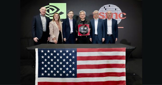
As Intel reportedly moves to bring 80–90% of Nova Lake compute tile production back in-house on its 18A process, TSMC is stepping up its U.S. expansion with advanced nodes including 2nm and beyond. The foundry giant added US$100 billion to its investment plan last week, raising its total U.S. commitment to US$265 billion — the largest foreign direct investment in U.S. history, according to KTAR News.
TSMC’s aggressive push reflects confidence in a “structural, multi-year demand” trend, with CFO Wendell Huang telling CNBC in a latest interview that the company has no intention of “leaving any food on the table.”
Behind TSMC’s U.S. Expansion
While CFO Wendell Huang told CNBC that the expansion reflects strong customer demand and supportive government policies, he also acknowledged the higher costs of overseas fabs. According to Huang, U.S. fab construction costs are roughly four to five times higher than those in Taiwan.
At last week’s earnings call, TSMC projected that overseas fab expansion would dilute gross margin by 2% to 3% in the early stages, with the impact widening to 3% to 4% in later stages. However, Huang emphasized that the investment would strengthen the U.S. semiconductor ecosystem and support long-term growth amid robust customer demand.
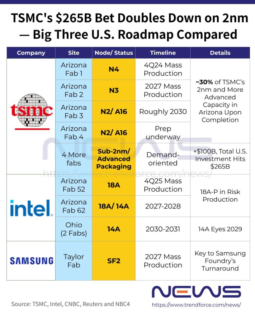
In another Reuters report, Huang provided an update on TSMC’s Arizona expansion. The first fab, built on 4nm, entered production in late 2024, while the second is set to begin equipment installation soon. Construction of the third fab is already underway, with preparatory work also kicking off for a fourth fab and the site’s first advanced packaging facility, Huang said.
As noted by City of Phoenix, TSMC’s first Arizona fab has been producing N4 chips at volume since late 2024, with yields now matching those achieved at the company’s Taiwan operations. Construction of the second fab, designed for 3nm production, has been completed, with volume manufacturing slated for 2027.
After the completion of its announced projects, Arizona will host about 30% of TSMC’s 2nm-and-beyond capacity, establishing a self-contained advanced semiconductor ecosystem in the U.S., according to City of Phoenix.
Once completed, TSMC’s current and planned Arizona projects will expand its U.S. footprint to a total of 12 wafer fabs and advanced packaging facilities, along with an R&D center, Reuters suggests.
Intel’s Nova Lake Shift Opens Opportunities for TSMC
Meanwhile, TSMC’s latest move comes as Intel’s 18A yields have reportedly increased sharply, reaching as high as 85% in the latest quarter, up from 65% previously, according to Wccftech. Commercial Times, citing supply chain sources, also adds that yields for Intel 18A client processors continue to improve, while the more complex Clearwater Forest server CPU has also entered early production.
Notably, the improved 18A momentum could also reshape the dynamics with TSMC. As Intel reportedly moves to bring Nova Lake compute tile production back in-house on 18A rather than relying on TSMC’s 2nm, the shift could free up advanced-node capacity at TSMC, creating new opportunities to serve other leading-edge customers, Commercial Times notes.
Among the potential beneficiaries, AMD is emerging as a key winner. The chipmaker is set to unveil its next-generation EPYC “Venice” server processors and Instinct AI accelerators this week, according to Commercial Times. As highlighted by the report, Venice will be among the first enterprise CPUs to adopt TSMC’s 2nm process, while the Instinct MI450, MI455, and upcoming MI550 series are also poised to become key products in AMD’s AI data center push.
Read more
- [News] Intel Might Build Up to 90% of Nova Lake Compute Tiles on 18A, Scaling Back TSMC’s Planned Role
- [News] TSMC Flags Four Key Challenges in Arizona Buildout Even as U.S. Fab Beats Expectations
(Photo credit: TSMC)


