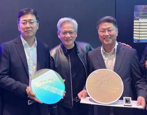
[News] China’s Prinano Claims 8-inch Photonic Chip Mass Production Using Nanoimprint Tech, Bypassing DUV Lithography
While China continues efforts to produce advanced chips without access to ASML’s EUV tools, it is also pushing to reduce reliance on DUV systems. According to the South China Morning Post, Chinese start-up Prinano claims it has validated mass production of photonic chips on 8-inch silicon wafers using nanoimprint technology, bypassing conventional lithography equipment altogether.
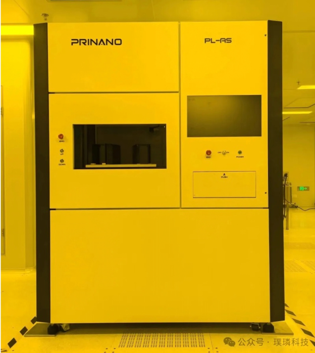
Instead of traditional optical lithography, Prinano relies on its proprietary PL-AS vacuum air-cushion nanoimprint lithography (NIL) platform. According to Tom’s Hardware, the company says the process can cut production costs to roughly one-tenth of conventional DUV-based methods while enabling wafer-scale photonic chip manufacturing.
Tom’s Hardware further notes that conventional semiconductor manufacturing typically relies on DUV or EUV systems, which use light to project circuit patterns onto silicon wafers. In contrast, nanoimprint lithography takes a different approach by directly stamping nanoscale structures onto a resist layer, eliminating much of the complex optical hardware used in traditional lithography, the report explains.
China AET, citing Prinamo’s announcement on WeChat, reports that the company’s PL-AS system supports sub-10nm line-width resolution, with wafer-scale pressure uniformity controlled within 0.5%. The platform also enables residue-free imprinting and offers alignment precision that can be tuned to sub-100nm levels.
Compared with conventional roll-based wafer-scale NIL, PL-AS applies uniform surface pressure across the entire wafer to ensure consistent force at every nanoscale point. This design reduces residual layer thickness (RLT) variation to below 2nm, while also offering higher throughput than Canon’s step-and-repeat NIL systems, which rely on sequential exposure rather than full-wafer compression, the report notes.
A Different Path for Nanoimprint Tech
Interestingly, Prinano is taking a more practical route, with no intention of competing in advanced processor or AI chip manufacturing. As highlighted by Tom’s Hardware, its commercialization efforts are focused on photonic semiconductors, which use light instead of electrical signals and are widely deployed in optical communications, data center interconnects, sensing systems, and LiDAR applications.
Industry observers generally see photonics as one of the most promising applications for nanoimprint lithography, as per Tom’s Hardware. Many of the key device structures rely on repetitive nanoscale patterns that can be efficiently replicated through imprinting, giving NIL a clearer path to commercialization compared with advanced logic chips, the report adds.
Prinano’s approach, which focuses on more mature technology nodes, contrasts with Japan’s broader nanoimprint ecosystem spanning both equipment and materials. According to Nikkei, Canon began commercializing nanoimprint lithography equipment in 2023, with systems priced at several billion yen (¥1 billion ≈ $6.4 million), significantly lower than EUV lithography tools.
The report also notes that Japan’s Dai Nippon Printing (DNP) is developing template materials for use with Canon’s equipment, targeting mass production from 2027 for 1.4nm chips.
Read more
- [News] TSMC Rejects High-NA EUV Investment Concerns, Confirms Purchase for R&D Use
- [News] China Reportedly Builds EUV Prototype Using Older ASML Components, Eyes 2028 Chipmaking
(Photo credit: Prinano)