[News] Nikon Targets Panel Packaging With New Lithography System Set for FY27 Launch, Targeting 30%+ Productivity Gain
While Nikon has lost ground in lithography competition with ASML, the Japanese equipment maker is stepping up efforts to diversify into emerging opportunities. According to a company press release, Nikon is targeting the panel-level packaging market through a new high-productivity digital lithography system designed to boost output by more than 30%.
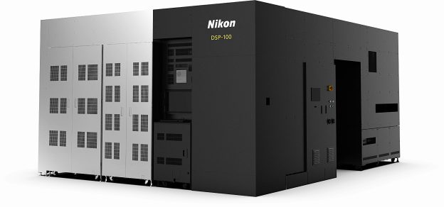
Nikon said that the system, scheduled for launch in fiscal year 2027, offers 1.5 µm resolution (L/S) and is designed to significantly improve throughput performance. Productivity is expected to rise by more than 30%, increasing output from 50 panels per hour with the DSP-100 system to 65 panels per hour or higher.
Beyond raw performance gains, Nikon emphasizes flexibility: by swapping the optical module, the system can also support 1.0 µm (L/S) resolution—matching the DSP-100—allowing customers to adapt to evolving process requirements and extend equipment lifecycle.
The strategy aligns with comments from CEO Yasuhiro Ohmura, who took office in April, in a previous Nikkei Asia interview. With ASML’s High-NA EUV systems reportedly costing up to $400 million per unit, Nikon is pushing a cost-down approach by increasing in-house component manufacturing to reduce overall system pricing and strengthen competitiveness, according to Nikkei.
Nikon’s ArF Lithography Tool Push
According to Nikkei, Nikon is in talks with several major chipmakers across the U.S. and Asia to supply argon fluoride (ArF) lithography tools, with some negotiations reportedly nearing purchase orders.
Nikkei explained that Nikon has long maintained close ties with Intel, which once accounted for up to 80% of its ArF lithography orders. However, the report added that sales have stalled in recent years amid challenges facing the U.S. chipmaker.
On the other hand, as highlighted by EE Times, Nikon also plans to launch a next-generation ArF immersion platform by 2028, featuring a new lens and wafer stage, while enhancing compatibility with ASML systems—an important factor for multi-tool process alignment in advanced fabs.
While ASML dominates EUV lithography, ArF immersion remains a critical segment of mature DUV processes, still widely used even in advanced nodes such as 3nm, the report notes.
(Photo credit: Nikon)


