[News] Intel Foundry Gains Momentum as Google Reportedly Orders 3M TPUs, NVIDIA Evaluates 18A for Multi-Die GPUs

Amid mounting capacity constraints and a widening shift among leading AI players to diversify their supply chains, Intel is emerging as a key beneficiary. Reuters and The Bull.com, citing The Information, report that Google has tapped Intel to manufacture more than 3 million TPUs in 2028, while NVIDIA is evaluating Intel’s 18A process and advanced packaging technologies for a next-generation multi-die GPU design.
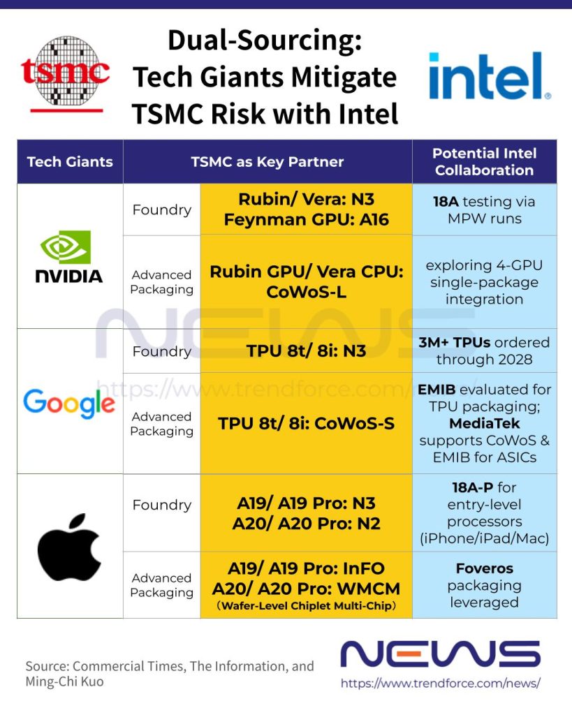
Intel Secures Major Google TPU Foundry Order
According to Guru Focus, the search giant is said to have placed orders for more than 3 million TPU chips with Intel through 2028, following extensive validation of its advanced packaging capabilities. In context, The Bull, citing Morgan Stanley estimates, notes that Google is expected to produce over 6 million TPUs between 2027 and 2028, implying that Intel’s foundry order could account for roughly half of its projected 2028 output.
If confirmed, the development would mark a further step forward for Intel’s foundry ambitions. Separately, an earlier Wccftech report indicated that Intel’s EMIB (Embedded Multi-die Interconnect Bridge) technology has reached yield levels of around 90%, with Google and Meta Platforms emerging as potential adopters in future designs. Citing analyst Jeff Pu, the report added that Google’s TPU v8e, expected in 2H27, is likely to incorporate Intel’s EMIB technology.
As highlighted by Reuters, Intel has already secured Tesla as the first major customer for its next-generation 14A process, which is expected to produce chips for Elon Musk’s planned Terafab AI computing hub in Austin.
NVIDIA Reportedly Tests Intel 18A for GPU Design
On the other hand, Futu News, citing The Information, reports that NVIDIA’s engagement with Intel remains at the evaluation stage, although the collaboration has moved beyond initial discussions. The AI accelerator leader is assessing whether Intel’s technology can support a new processor design that integrates four GPU dies into a single package, a development closely linked to NVIDIA’s next-generation Feynman GPU architecture, the report adds.
At the same time, NVIDIA has begun early testing of Intel’s 18A process through multi-project wafer (MPW) runs, a cost-sharing model that allows multiple customers to place small chip designs on the same wafer to validate manufacturing feasibility, according to Futu News.
NVIDIA’s broader engagement with Intel highlights potential shifts in the competitive foundry landscape, where TSMC currently remains the company’s primary manufacturing and advanced packaging partner. NVIDIA’s Rubin GPUs are being produced on TSMC’s 3nm process with CoWoS advanced packaging, while earlier reports from Commercial Times suggested that its next-generation Feynman architecture is expected to be manufactured using TSMC’s A16 process.
Still, Intel maintains a complex coopetition relationship with TSMC, as the compute die of Nova Lake, scheduled for 2H26, is reportedly being outsourced to TSMC’s 2nm process, according to Tom’s Hardware.
Read more
- [News] Intel Says 18A May Reach Strong Margins by 2027; Notebook Chips on the Node Mark Fastest Ramp in 5 Years
- [News] Intel Reportedly to Adopt Silicon Capacitors in 2027 to Improve EMIB Power Stability for Google’s v8e
(Photo credit: Intel’s X)


