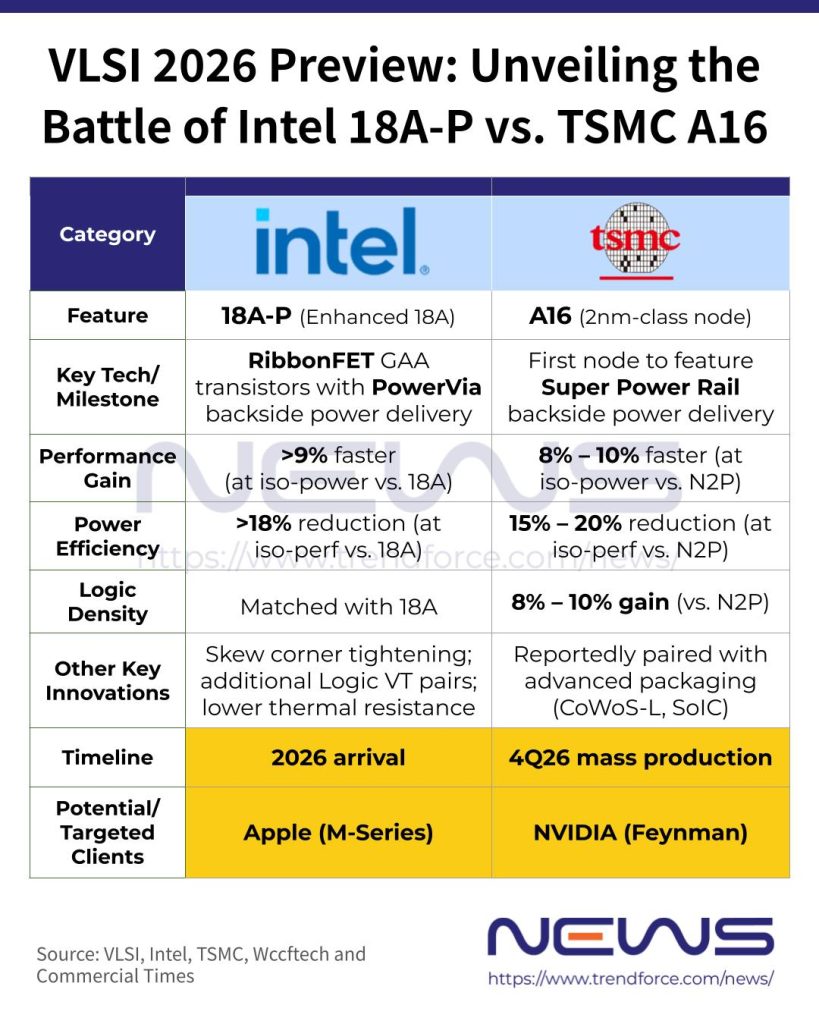
[News] Intel 18A-P and TSMC A16 Set for VLSI Showdown in Advanced Node Push: 18% Power Savings vs SPR Debut
Market chatter continues to link Apple as a potential early adopter of Intel’s 18A-P for future M-series chips, with more technical details expected to surface at the VLSI Symposium in mid-June. Based on information disclosed on the VLSI website, Intel’s enhanced 18A-P process delivers over 18% lower power at the same performance level, or more than 9% higher performance at equivalent power compared with standard 18A.
Against this backdrop, the VLSI Symposium is also shaping up as a key battleground between Intel and TSMC at the advanced nodes. TSMC is set to unveil its 2nm-class A16 Angstrom CMOS technology, featuring gate-all-around (GAA) transistors and backside power delivery via its new “Super Power Rail” (SPR) design, according to VLSI technical highlights.
Intel Offers First Spoiler on 18A-P
As reported by Wccftch, Intel noted that key structural parameters in 18A-P, including Library Height and Contacted Poly Pitch, remain unchanged from the base 18A node. The enhancements, as per the report, instead focus on transistor-level tuning and voltage optimization, including expanded BT pair options at 5+ for VT (threshold voltage) versus four in 18A, and the introduction of a new Logic VT positioned between ULVT (ultra-low threshold voltage) and LVT (low threshold voltage).
Separately, Tom’s Hardware highlights that 18A-P brings tighter process variability control alongside improved thermal efficiency, contributing to higher performance at lower power levels. These refinements are also seen as potential factors behind growing interest from Apple and other fabless chip designers, according to the report.
To achieve these gains, the report suggests Intel introduced new gate-all-around RibbonFET variants, including enhanced-contact high-performance transistors and optimized low-power devices, providing the device-level foundation for improved performance and power efficiency.
Notably, Wccftech, citing Intel, also reports that the company has tightened skew corners by 30% in 18A-P, a move aimed at improving performance consistency and reducing variability. As explained by EXP review, “skew corners” refer to the spread in performance and power characteristics between transistors on the same process node. As semiconductor manufacturing scales to more advanced nodes, transistor behavior becomes increasingly non-uniform, making variability control a critical factor.
While Intel’s first 18A-based product, Panther Lake, entered mass production in late 2025, the company had previously indicated that its 18A derivatives would follow in phases. According to TechNews, 18A-P is expected to arrive around 2026, with the further enhanced 18A-PT targeted for 2028.
TSMC Sets Stage for A16 Debut at VLSI
Meanwhile, TSMC is expected to unveil its first Super Power Rail-based node, A16, at the VLSI Symposium scheduled for June 14–18. According to the company, compared with its performance-enhanced N2P node, A16 is projected to deliver 8%–10% higher performance at the same power level, or cut power consumption by 15%–20% at equivalent performance, while also improving chip density by an additional 8%–10%.
TSMC is targeting mass production of its A16 process in the fourth quarter of 2026, with NVIDIA’s Feynman widely rumored to be the first adopter. As previously reported by Commercial Times, A16 is positioned as a key solution for HPC workloads. Supply chain sources cited by the report indicate the node will be paired with CoWoS-L and SoIC advanced packaging technologies, enabling system scaling of up to 9.5× reticle size.
Read more
- [News] Intel Foundry Gains Momentum: Apple Reportedly Eyes 18A-P as Google Explores Advanced Packaging
- [News] Intel Fab 52 Reportedly Rivals TSMC Arizona Phase 1 and 2 Combined Capacity on More Advanced 18A
(Photo credit: Intel)