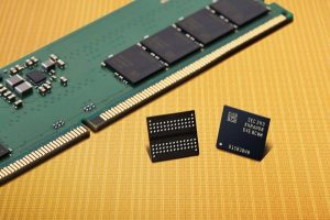
[News] Kioxia, SanDisk to Demonstrate QLC NAND Using Multi-Stacked Cell Architecture, Targeting 1,000+ Layers
As memory makers accelerate migration toward ~300-layer class NAND, Kioxia and SanDisk are reportedly pushing further ahead. According to EE Times Japan, the companies have achieved a world-first demonstration of quad-level cell (QLC) operation using a multi-stacked cell array CMOS (MSA-CBA) architecture enabled by wafer-to-wafer Cu direct bonding—seen as a key step toward ultra-high-density 3D NAND exceeding 1,000 layers.
The report notes that Kioxia and SanDisk will jointly present the breakthrough at the 2026 VLSI Symposium in Hawaii during June 14–18, adding that the two memory leaders say the advance overcomes key challenges in 3D NAND scaling, including cell current degradation, wafer warpage, and large block (BLK) size constraints.
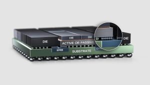
As explained by the report, in pre-released technical highlights, Kioxia and SanDisk showcased schematic diagrams of the MSA-CBA (Multi-Stacked Cell Array – CMOS Bonded Architecture) device structure illustrating sequential stacking and bonding, along with FIB-SEM (Focused Ion Beam – Scanning Electron Microscope) images of stacked cell arrays formed by two 218-word-line array wafers.
Notably, as previously reported by BLOCKS & FILES, Kioxia already outlined a roadmap toward 1,000-layer 3D NAND in 2024. Citing Japanese media outlet PC Watch, the report added that Kioxia projects NAND die density could reach 100 Gbit/mm² alongside 1,000-wordline 3D NAND by 2027.
According to BLOCKS & FILES, 3D NAND layer counts have expanded from around 24 layers in 2014 to 238 layers in 2022—roughly a tenfold increase over eight years. Kioxia’s model assumes a continued ~1.33× annual scaling pace, making the 1,000-layer milestone by 2027 technically plausible under current trajectories. The latest breakthrough, set to be unveiled at the 2026 VLSI Symposium, appears to offer an encouraging early signal that this roadmap remains firmly on track.
Samsung on 1000-Layer NAND
Notably, while taking a more measured approach, Samsung Electronics has previously outlined their paths toward 1,000-layer NAND. As reported by The Bell in 2025, Samsung unveiled its multi-BV NAND concept at the International Solid-State Circuits Conference in San Francisco, featuring two cell wafers stacked atop two peripheral wafers for 1,000-layer scaling. The report noted the architecture bears strong similarities to Kioxia’s Multi-Stack CBA (CMOS directly Bonded to Array) approach.
According to the report, industry estimates suggested a single wafer can support roughly 500 NAND layers when dedicated solely to cell structures, making multi-wafer stacking increasingly essential for reaching the 1,000-layer milestone. At Samsung Tech Day 2022 in Silicon Valley, the memory giant formally laid out its roadmap to develop 1,000-layer NAND by 2030, The Bell noted.
It is interesting to note that Samsung is also actively experimenting with new materials and architectures in its push forward. According to SeDaily, researchers from Samsung Semiconductor Research, NVIDIA, and Georgia Tech jointly introduced the PINO (Physics-Informed Neural Operator) AI model, which can analyze ferroelectric NAND performance up to 10,000× faster than conventional simulation methods.
The report adds that ferroelectric NAND is emerging as a next-generation candidate, potentially enabling up to 1,000 stacked layers while cutting power consumption by as much as 96%, addressing both supply constraints and energy efficiency demands.
Read more
- [News] Kioxia, TEL and Photoresist Makers in Focus After Magnitude 7.7 Japan Earthquake; Supply Chain Impact Mixed
- [News] Kioxia Reportedly Exits 2D NAND Market, Phasing Out Floating Gate and BiCS FLASH Gen 3 in 2028
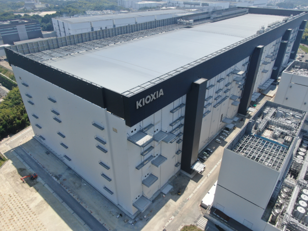
(Photo credit: Kioxia)