[News] Kioxia, TEL and Photoresist Makers in Focus After Magnitude 7.7 Japan Earthquake; Supply Chain Impact Mixed
A magnitude 7.7 earthquake struck off Japan’s northeastern coast on April 20, putting renewed focus on potential disruptions to the semiconductor supply chain, given the region’s concentration of key memory production and chipmaking materials and equipment suppliers.
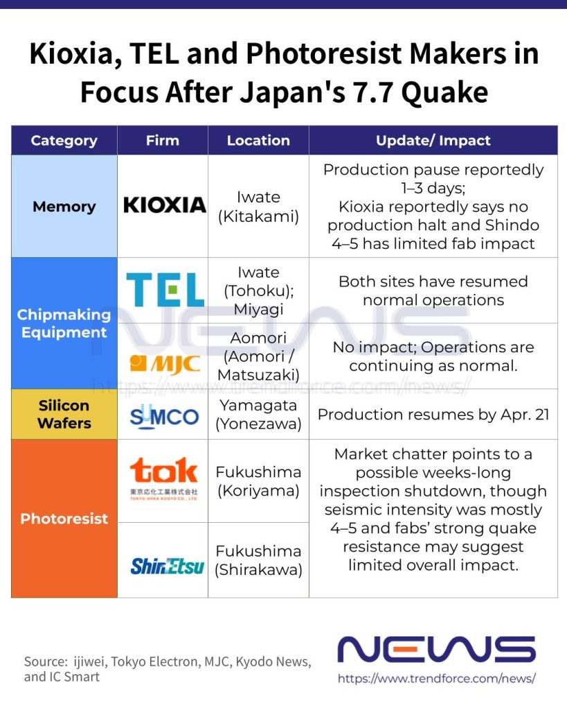
According to ijiwei, Kioxia has suspended production at its Iwate NAND facilities following the quake, while initial inspections are expected to take one to three days. Against this backdrop, below is a quick roundup of how Japan’s major semiconductor players are being affected by the earthquake.
Earthquake Brings Kioxia Iwate Operations into Focus
According to Yahoo! Japan, the earthquake struck at 4:53 p.m. on Monday, with its epicenter located off the Sanriku coast. The report suggests that at the highest recorded level, Shindo 5+ (Strong) was observed in Hashikami-cho in Aomori Prefecture, making it the single hardest-hit municipality in this event.
Notably, ijiwei explains that the affected area spans Iwate, Aomori, Miyagi, and Fukushima prefectures—home to major global players including Kioxia, Tokyo Electron, Shin-Etsu Chemical, and SUMCO. TechNews adds that while no major semiconductor fabs are currently located in areas that recorded seismic intensity of upper or lower 5, regions that experienced intensity 4 include facilities such as Kioxia’s Kitakami plant.
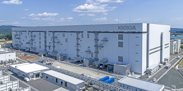
According to ijiwei, Kioxia’s Fab 1 and Fab 2 plants in Kitakami—key NAND production sites accounting for an estimated 5% to 8% of global capacity—have come under close scrutiny following the quake. As per the report, no major structural damage has been reported so far. That said, inspections are expected to take one to three days, while the timing for a full resumption of operations remains uncertain, ijiwei notes.
However, as per IC Smart, a source from Kioxia reportedly said no production halt and Shindo 4–5 has limited fab impact.
Notably, as previously reported by EE Times Japan, Kioxia’s K2 fab is built with a seismic isolation structure designed to absorb earthquake tremors. At the K2 site, production will center on high-density 218-layer 3D NAND using CBA (CMOS directly Bonded to Array) technology, with full-scale shipments slated to begin in the first half of 2026, according to the report.
Seismic Shaking Extends to Hokkaido
On the other hand, Yahoo! Japan reports that Shindo 4 shaking was also observed in Hokkaido, marking the northernmost extent of significant tremors from this earthquake. TechNews notes that Hokkaido has in recent years emerged as Japan’s third major semiconductor hub, adding that government-backed foundry Rapidus is currently building a new fab in Chitose, targeting 2nm mass production by 2027—raising potential follow-on impact concerns.
In contrast, Kyushu—where Sony, ROHM, and TSMC’s Kumamoto fab are located—recorded only seismic intensity levels of 1 to 2 and has not been directly impacted, ijiwei suggests.
TEL and Wafer Makers See Limited Impact
On the other hand, ijiwei reports that Tokyo Electron’s Tohoku production and logistics center in Oshu, Iwate Prefecture, was fully evacuated and temporarily shut down following the quake. Inspections are reportedly underway, focusing on equipment alignment, mechanical precision, and potential damage to piping and electrical systems.
However, in a separate press release on April 20, Tokyo Electron stated that no structural damage was found at its Tokyo Electron Technology Solutions Tohoku Plant and Tokyo Electron Miyagi facilities. Both sites have resumed normal operations.
Ijiwei adds that wafer suppliers have proactively paused operations for checks as well, as Shin-Etsu Chemical and SUMCO suspended production at their 12-inch wafer fabs in Miyagi and Fukushima to conduct safety inspections on equipment and wafers. According to EE Times China, both companies are expected to gradually resume production from April 21, and given the currently relatively ample global supply of silicon wafers, the impact of the shutdown is expected to be limited.
Photoresist Supply Under Pressure
Notably, ijiwei highlights potential pressure on the photoresist segment following the quake. As per the report, Tokyo Ohka Kogyo (TOK) has placed its Koriyama plant in Fukushima—accounting for roughly 25% of global advanced photoresist capacity—under a full shutdown for comprehensive inspections, with downtime expected to last four to six weeks.
Meanwhile, the report adds that Shin-Etsu Chemical has also suspended operations at its Shirakawa facility in Fukushima, where equipment recalibration is expected to take four to eight weeks.
As reported by ijiwei, Kioxia’s brief inspection-related pause at its NAND fabs could trigger short-term supply fluctuations in tightly balanced segments such as AI servers and automotive memory. In contrast, impacts on silicon wafers and semiconductor equipment are expected to remain limited.
However, the photoresist segment stands out as the most exposed area, given its high concentration of advanced capacity. The duration and pace of production restarts at key suppliers are therefore emerging as the critical variables to watch, the report notes.
Read more
- [News] Kioxia Reportedly to Make 332-Layer 10th-Gen NAND at Kitakami in 2026, Repurposing Existing Fab
- [News] Japan Earthquake Impact: TEL and Rapidus Unharmed, Spotlight Turns to Kioxia Kitakami Fabs
(Photo credit: Kioxia)


