[News] Semiconductor Packaging and Testing Capacity Race Intensifies as ASE, Samsung and Amkor Announced New Moves
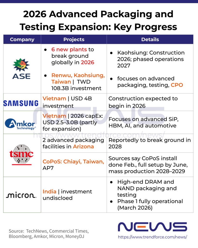
Since April 2026, global semiconductor packaging and testing sector has seen a wave of major developments. ASE has kicked off its largest-ever fab construction program, with six new facilities slated to break ground worldwide this year. Meanwhile, Samsung Electronics plans to invest USD 4 billion in a new packaging and testing plant in Vietnam, while Amkor is simultaneously accelerating its capacity expansion in the country.
ASE Expands Production Globally
On April 10, 2026, ASE Technology Holding held a groundbreaking ceremony for a new facility in Kaohsiung’s Renwu Industrial Park. With total investment exceeding TWD 108.3 billion, the plant will focus on advanced semiconductor testing services, covering applications such as AI, HPC, 5G communications, and automotive electronics. Phase one is scheduled to be completed by April 2027, followed by phase two in October the same year. The facility is expected to generate annual output value of up to TWD 177.3 billion.
This project represents only part of ASE’s broader global expansion. According to CEO Tien Wu, 2026 marks the company’s most aggressive year for fab construction, with six new plants expected to break ground worldwide—a record high. In addition to the Kaohsiung site, expansion projects span the United States, Malaysia, Japan, and Germany, aimed at addressing AI-driven semiconductor demand growth.
In terms of capital expenditure, ASE initially budgeted USD 7 billion for 2026 but indicated potential upward revision due to robust market demand, with details to be disclosed in its upcoming earnings call.
On the technology front, Wu noted that co-packaged optics (CPO) is set to enter mass production in 2026. To support rapid expansion, ASE has also launched a new round of hiring, targeting 3,000 technical recruits in 2026 and an additional 1,000 in 2027 to bolster R&D and capacity ramp-up.
Samsung and Amkor Bet on Vietnam
According to Bloomberg on April 10, Samsung Electronics plans to invest USD 4 billion to build a semiconductor packaging and testing facility in Thai Nguyen Province, northern Vietnam, with an initial phase investment of USD 2 billion. This would mark Samsung’s largest single investment in the segment since entering Vietnam in 2008. Vietnam’s Ministry of Finance has confirmed ongoing discussions with Samsung regarding semiconductor investment cooperation.
The new facility will be located near Samsung’s existing smartphone manufacturing base, leveraging the region’s established supply chain and infrastructure to meet rising global demand for chip packaging and testing driven by data centers and AI devices.
Industry observers note that Samsung’s move aligns with ongoing investments by TSMC and Intel in advanced packaging, reinforcing its position across the semiconductor value chain. Vietnam, benefited from competitive labor costs, strategic location, and an established industrial base, is increasingly emerging as a key destination for packaging and testing capacity relocation.
Meanwhile, Amkor is accelerating expansion of its Vietnam operations. Since 2021, the company has invested a cumulative USD 1.6 billion to build advanced packaging facilities in the Yen Phong 2C Industrial Park in Bac Ninh Province. This site represents Amkor’s largest advanced packaging base globally, focusing on system-in-package (SiP) and HBM memory integration, and offering turnkey solutions from design to electrical testing.
According to Amkor’s February 2026 financial report, the company plans capital expenditures of USD 2.5–3.0 billion for the year, primarily targeting advanced packaging capacity expansion, including its Vietnam operations. Key end markets include HPC, AI, automotive electronics, IoT, and mobile communications.
Vietnam has been positioned by Amkor as a “growth engine for the next decade,” aimed at diversifying supply chain risks. Its Vietnam facilities adopt a modular production layout with 25% reserved capacity flexibility, enabling rapid equipment reconfiguration in response to policy or market changes.
Competition in Semiconductor Packaging and Testing Sector Heats up
Semiconductor packaging and testing constitute the back-end processes of chip manufacturing, encompassing two main stages: packaging and testing. Packaging involves processes such as dicing, die attach, wire bonding or flip-chip, and molding, providing physical protection, electrical interconnection, thermal management, and standardized interfaces for chips. Testing includes wafer probing (CP) and final testing (FT), using specialized equipment to identify defective or underperforming chips, ensuring product quality and reliability before shipment.
As Moore’s Law effect slows, advanced packaging has become a critical pathway for enhancing chip performance, while the value contribution of testing continues to rise alongside increasing chip complexity. Since the start of 2026, multiple companies worldwide have announced new or expanded packaging and testing facilities.
(Photo credit: ASE)


