[News] SK hynix Reportedly Weighs TSMC 3nm for HBM4E Logic Dies to Gain Edge over Samsung
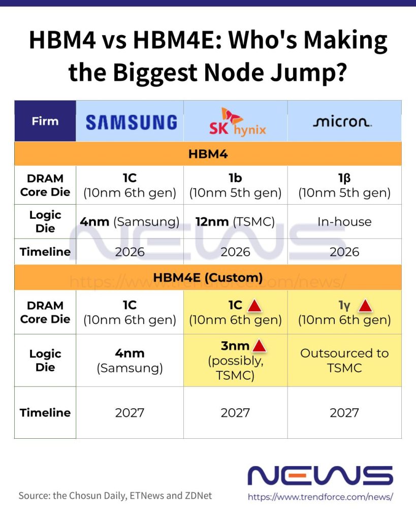
With all three leading memory giants now close to shipping HBM4, the race for next-gen HBM is intensifying, with advanced nodes taking center stage. Samsung is reportedly set to use its in-house 4nm process for HBM4E logic dies, while SK hynix, according to the Chosun Daily, is considering TSMC’s 3nm technology for its HBM4E logic dies.
As previously reported by ETNews, Hwang Sang-jun, Vice President and Head of Memory Development at Samsung Electronics, said that the base die of HBM5 will adopt Samsung Foundry’s 2nm process, compared with the 4nm base dies used in HBM4 and HBM4E.
If confirmed, SK hynix’s move appears aimed at gaining a performance edge by applying advanced nodes not only to HBM’s stacked DRAM but also to the logic dies handling computation.
The Chosun Daily further notes that SK hynix is expected to adopt a 10nm-class 6th-generation (1c) DRAM process for the core die used in HBM4E, while applying TSMC’s 3nm to the logic die. For the HBM4 supplied to NVIDIA this year, the company reportedly uses a 10nm-class 5th-generation (1b) DRAM core die alongside a logic die based on TSMC’s 12nm. In contrast, Samsung has equipped its HBM4 with a 1c DRAM core die and a logic die built on 4nm.
Custom HBM Takes Off with HBM4E
The Chosun Daily highlights that with HBM4E, the custom HBM market—where logic dies are tailored to client-specific circuit requirements—is expected to fully take off. This could bring a variety of foundry nodes into play, though SK hynix appears focused on a 3nm-based strategy, the report adds.
An industry insider cited by the report noted that HBM4E logic dies are designed to client specifications, so multiple process nodes—including 3nm and 12nm—are being considered. Still, 3nm is expected to dominate most HBM4E logic dies. The report adds that HBM4E is slated for NVIDIA’s next-gen AI chip, Vera Rubin Ultra.
More details for custom HBM logic dies have also surfaced. TechPowerUp reported in late 2025 that TSMC’s C-HBM4E logic die will transition from the current 12 nm HBM4 logic dies to the N3P node, cutting voltage from 0.8 V to 0.75 V.
Read more
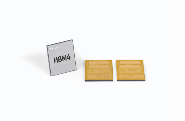
(Photo credit: SK hynix)