Popular Keywords
About TrendForce News
TrendForce News operates independently from our research team, curating key semiconductor and tech updates to support timely, informed decisions.
[News] Hybrid Bonding Leader BESI Reportedly Draws Takeover Interest; Lam, Applied Materials Rumored
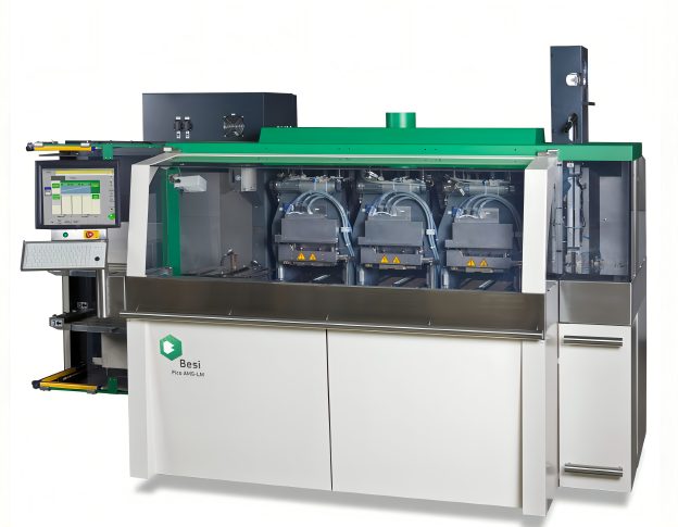
BESI, an industry leader in hybrid bonding technology critical to HBM packaging, is reportedly attracting takeover interest. According to Reuters, sources say BE Semiconductor (BESI) has received takeover approaches as demand for its chip-packaging technology has become increasingly important for semiconductor equipment makers. The company is said to be working with an investment bank to evaluate the approaches, the report adds.
As the report highlights, U.S. chip-equipment maker Lam Research is among the suitors that have held discussions with BESI. Other potentially interested parties include equipment manufacturer Applied Materials, which acquired a 9% stake in BESI in April last year and became its largest shareholder. The report also notes that BESI and Applied Materials have been long-term partners in hybrid bonding. The technology directly links chips through copper-to-copper connections, enabling faster data transfer and lower power consumption in advanced semiconductors.
Dutch equipment maker BESI is widely regarded as the leading company in hybrid bonder technology, Hankyung indicates. While the company currently holds the top position in hybrid bonder equipment, competition is beginning to emerge. The report notes that several Korean companies including LG Electronics, SEMES, Hanmi Semiconductor and Hanwha Semitech are developing related systems, while Singapore-based ASMPT is also working to build capabilities in the technology.
HBM Thickness Debate Puts BESI’s Hybrid Bonding Strategy in Focus
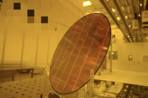
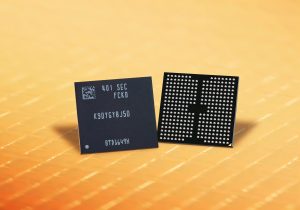
Meanwhile, aside from takeover rumors, Besi has also recently come under the spotlight amid potential changes to HBM thickness standards. As noted by Wall Street Journal, citing ZDNet, the Joint Electron Device Engineering Council (JEDEC)—an industry body for microelectronics whose members include NVIDIA—is considering relaxing thickness standards for next-generation HBM stacks. The report notes that such a move could delay hybrid bonding adoption, as chipmakers could continue using thermocompression (TC) bonding, a cheaper and proven technology that joins chips through soldering.
As noted by Investing.com, the implications for BESI are direct. If thickness standards are relaxed, chipmakers may face less urgency to move beyond existing bonding equipment. This could slow the shift toward hybrid bonding, which is a more precise but also more expensive process that lies at the core of BESI’s long-term growth strategy.
Read more
- [News] Applied Materials Teams Up with Micron, SK hynix for Next-Gen DRAM, HBM and NAND Development
- [News] Industry Weigh 825–900 μm HBM Thickness for 20-High Stacks, Potentially Slowing Hybrid Bonding
(Photo credit: BESI)
Please note that this article cites information from Reuters, Hankyung, Wall Street Journal, ZDNet, and Investing.com.