Popular Keywords
About TrendForce News
TrendForce News operates independently from our research team, curating key semiconductor and tech updates to support timely, informed decisions.
[News] SK hynix Reportedly Accelerates Hybrid Bonding for 300-Layer V10 NAND, Eying 2027 Mass Production
SK hynix is pushing its NAND technology forward with the adoption of hybrid bonding. According to Hankyung, the company is developing 300-layer NAND that incorporates this process, joining other leading manufacturers—Samsung Electronics, China’s YMTC, and Japan’s Kioxia—in moving toward full-scale hybrid-bonding deployment.
Sources cited by the report indicate that SK hynix is working on its 10th-generation (V10) NAND at the 300-layer level and aims to complete development through the pilot line next year, before moving into full production early the year after.
Hybrid Bonding Becomes the Defining Shift in SK hynix’s V10 NAND
As the report notes, V10’s standout feature is SK hynix’s first deployment of hybrid bonding, a process that joins two semiconductor wafers so they function as a single unit.
Up through V9 (321 layers), SK hynix produced both the cell array and peripheral circuitry on a single wafer. As the report indicates, under the PUC (Peri-under-Cell) scheme, the peripheral circuits were positioned at the bottom of the wafer, with the memory layers stacked directly above them.
This configuration, however, exposes the peripheral circuits to greater risk. The report notes that hybrid bonding alleviates this issue and can even shorten production time, since the peripheral and cell wafers are fabricated separately.
Meanwhile, the report also points out that hybrid bonding increases process complexity, and the hybrid bonding tools required for wafer-to-wafer integration are largely supplied by Austria’s EVG and Japan’s Tokyo Electron.
Global NAND Makers Speed Up the Hybrid Bonding Shift
While the industry anticipated SK hynix would adopt hybrid bonding beyond 400 layers, the report notes that the company is applying it at the 300-layer V10 stage in response to competitors’ faster commercialization.
For instance, the report notes that Japan’s Kioxia adopted hybrid bonding in 2023 through its CBA (CMOS Directly Bonded to Array) architecture, while Samsung Electronics plans to introduce the technology with its upcoming V10 device (around 400 layers), which is expected to enter mass production soon, according to the report.
SK hynix Ramps Up Production Amid Surging SSD Demand
Meanwhile, the report also notes that SK hynix will continue investing next year in both V10 development and the conversion of existing tools to expand V9 production. An industry source cited by the report said that although SK hynix was still building NAND inventory in the first half of the year, rising enterprise SSD demand has since pushed its fabs close to full capacity.
The report adds that SK hynix’s highest-stacked mass-produced NAND is currently the 321-layer V9, which supports the company’s position as the No. 2 player in the global NAND market.
Read more
- [News] SK hynix Reportedly Eyes 321-Layer QLC NAND in 2H26; Future of Solidigm IPO Uncertain
- [News] SK hynix Unveils Organizational Restructure with Dedicated HBM Taskforce in the Americas
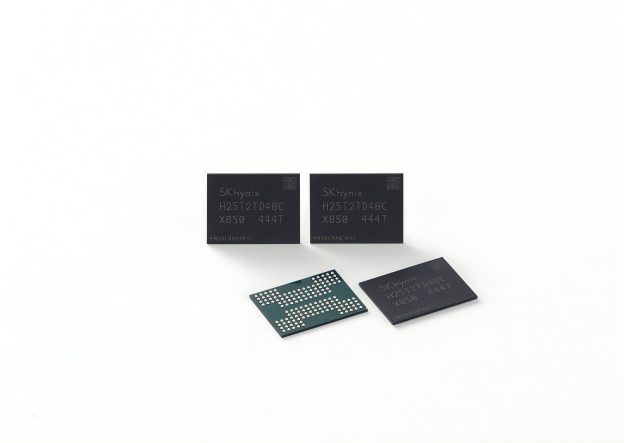
(Photo credit: SK hynix)
Please note that this article cites information from Hankyung.