Popular Keywords
- About Us
-
Research Report
Research Directory
Semiconductors
LED
Consumer Electronics
Emerging Technologies
- Selected Topics
- Membership
- Price Trends
- Press Center
- News
- Events
- Contact Us
- AI Agent
About TrendForce News
TrendForce News operates independently from our research team, curating key semiconductor and tech updates to support timely, informed decisions.
- Home
- News
[News] TSMC Unveils Custom C-HBM4E Details: N3P Logic Dies Reportedly Target 2× Efficiency Gain

As memory makers push deeper into custom HBM logic dies for the HBM4 era, foundries—led by TSMC—are stepping up with more breakthroughs. German outlet HardwareLUXX reports that TSMC’s custom HBM4E, currently dubbed C-HBM4E, will leap to the N3P node. Along with dropping voltage from 0.8 V to 0.75 V, TSMC says the new process delivers 2× the power efficiency of today’s DRAM manufacturing, the report notes.
The report—citing TSMC’s presentation at last week’s Open Innovation Platform Ecosystem Forum in Amsterdam—notes that even the base dies will see notable upgrades in the HBM4 era thanks to the foundry giant’s more advanced processes. Instead of relying on a standard DRAM process as in HBM3E, TSMC plans to build HBM4 base dies on its N12 node, cutting operating voltage from 1.1 V to 0.8 V, the report adds. According to HardwareLUXX, this shift is expected to deliver an efficiency gain of roughly 1.5×.
Notably, HardwareLUXX highlights that for C-HBM4E, in addition to the leap with TSMC’s N3P, the base die will also integrate memory controllers—components typically housed in the host chip to which HBM connects—meaning the physical interface (PHY) will also be a custom solution.
Meanwhile, TSMC is pulling in major orders for its custom HBM logic-die solutions. Tom’s Hardware reports that Micron has tapped TSMC to fabricate the base logic die for its HBM4E, targeting 2027 production. SK hynix—another key TSMC partner on custom HBM—is expected to roll out its first tailored offering, HBM4E, in the second half of next year, according to industry sources cited by Korea Economic Daily.
Notably, Korea Financial Times reports that SK hynix will deploy TSMC’s 12nm process for mainstream server base dies while escalating to 3nm for premium designs targeting NVIDIA’s flagship GPUs and Google’s TPUs.
Read more
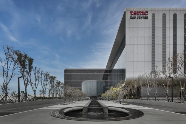
(Photo credit: TSMC)


