Popular Keywords
About TrendForce News
TrendForce News operates independently from our research team, curating key semiconductor and tech updates to support timely, informed decisions.
[News] Intel Advanced Packaging Reportedly Gains Traction, with Apple and Qualcomm Seeking EMIB Expertise
While TSMC has long dominated the advanced packaging landscape, Team Blue’s technology is reportedly gaining traction. According to Wccftech, Intel’s EMIB and Foveros technologies are seeing growing interest, with Apple and Qualcomm posting job openings seeking talent experienced in its EMIB packaging. While these listings don’t necessarily confirm adoption of Intel’s solutions, but they signal rising industry interest in the company’s advanced packaging offerings, the report adds.
Interest in Intel’s advanced packaging is rising in part because TSMC is facing capacity bottlenecks, with its advanced packaging lines heavily booked by major customers such as NVIDIA and AMD. As companies like Apple, Qualcomm, and Broadcom ramp up their custom-silicon efforts, they are increasingly exploring Intel’s alternatives, the report highlights.
Intel’s Advanced Packaging Push: EMIB, Foveros, and U.S. Expansion
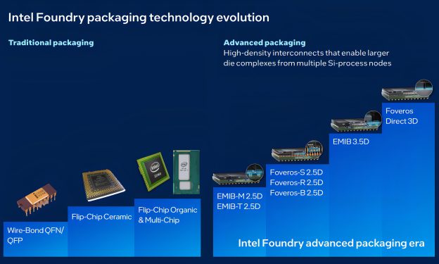
As the report explains, EMIB (Embedded Multi-Die Interconnect Bridge) allows multiple chiplets to be linked within a single package through a small embedded silicon bridge, removing the need for a large interposer, unlike TSMC’s CoWoS. Building on EMIB, Intel also offers its Foveros Direct 3D packaging technology, which enables die stacking on a base die using through-silicon vias (TSVs).
As noted by TechPowerUp, EMIB is a substrate-embedded silicon bridge that enables localized, high-density die-to-die routing without the cost and area overhead of a full silicon interposer. Small EMIB bridges can deliver low-cost, high-density shoreline connections, making them well suited for logic-to-logic and logic-to-HBM interfaces.
The EMIB variants give chip designers considerable flexibility across different package types and make it possible to pursue far more complex architectures than traditional approaches allow. TechPowerUp adds that this capability enhances Intel Foundry’s overall value proposition, making its advanced packaging technologies increasingly appealing to ASIC developers seeking higher performance and more sophisticated multi-die designs.
Notably, Intel is expanding its advanced packaging capacity in the U.S., as TechPowerUp notes. The company has long relied on global sites such as the Pelican plant in Malaysia for parts of its packaging work, but in early 2024 it began upgrading its New Mexico facilities to support more advanced packaging. The Fab 9 and Fab 11x sites in Rio Rancho are now the first to mass-produce Intel’s 3D advanced packaging technologies.
Read more
- [News] Intel Reportedly Kills Off 8-Channel Diamond Rapids as Server Market Shifts to High-Capacity
- [News] Intel CTO and AI Chief Departs for OpenAI; CEO Lip-Bu Tan Steps In to Lead AI Push
(Photo credit: Intel)
Please note that this article cites information from Wccftech and TechPowerUp.