Popular Keywords
About TrendForce News
TrendForce News operates independently from our research team, curating key semiconductor and tech updates to support timely, informed decisions.
[News] FOPLP Trial Yields Reportedly Reach 90% at Powertech as TSMC Advances CoPoS Development
As semiconductor heavyweights spearheaded by TSMC accelerate panel-level fan-out packaging (FOPLP) development to revolutionize chip packaging efficiency, the technology is gaining significant traction. According to Commercial Times, supply chain sources reveal that FOPLP production equipment has been successfully shipped, with customer pilot programs delivering impressive 90% yield rates.
As Commercial Times explains, by replacing wafers with square panels, industry players are pursuing a dual-track approach in terms of FOPLP. On one front, FOPLP has reportedly entered small-scale production, with Taiwan’s Innolux and Powertech Technology taking the lead in packaging smaller chips such as PMICs and power components.
Meanwhile, TSMC is charting its own course with CoPoS (Chip on Panel on Substrate), targeting tech titans NVIDIA and AMD for larger, GPU-centric applications, the report suggests.
Commercial Times notes that today’s rectangular carriers for FOPLP mainly use metal or glass substrates, with mainstream sizes ranging from 310×310mm at TSMC and 515×510mm at Powertech, to 600×600mm at ASE and 700×700mm at Innolux. The report adds that Powertech, after deploying next-gen laser and creamy equipment, has already pushed its FOPLP line to a 90% trial yield, with expectations of surpassing 95% next year.
Industry insiders point out that unlike FOWLP (Fan-Out Wafer-Level Packaging), which uses wafers, FOPLP adopts rectangular carriers. At 600×600mm², a single panel offers more than five times the area of a 12-inch wafer, while utilization jumps from about 57% to 87%—cutting unit costs and improving production flexibility, the report suggests.
TSMC’s CoPoS Push
On the other hand, Commercial Times notes that TSMC has set up dedicated FOPLP R&D teams and lines, investing in PLP (Panel Level Packaging) and TGV (Through-Glass Via) to advance glass substrate development. While mass production was originally slated for 2027, supply chain sources now suggest the timeline could be pulled forward.
Notably, TSMC confirmed in August it will phase out 6-inch wafer production within two years and consolidate 8-inch capacity to boost efficiency. According to Liberty Times, whether Fab 2 (6-inch) and Fab 5 (8-inch) will be repurposed for advanced packaging still requires further evaluation. However, recent rumors suggest TSMC may convert these fabs to CoPoS production.
Read more
- [News] FOPLP Heats Up: ASE, Powertech Expand; TSMC Reportedly Preps 2026 CoPoS Pilot Line
- [News] TSMC Reportedly Gears Up for CoPoS Mass Production by 2029, Tapping NVIDIA as First Client
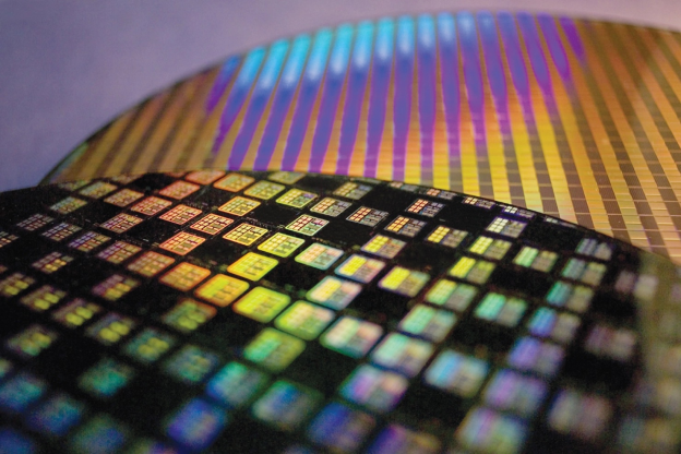
(Photo credit: TSMC)
Please note that this article cites information from Commercial Times and Liberty Times.