Popular Keywords
About TrendForce News
TrendForce News operates independently from our research team, curating key semiconductor and tech updates to support timely, informed decisions.
[News] Memory Giants SanDisk, SK hynix Unite for HBF Standard, with Samples Expected in 2H26
U.S. NAND leader Sandisk, fresh off launching a Technical Advisory Board to guide its groundbreaking High Bandwidth Flash (HBF) technology in July, has now signed a landmark MoU with South Korean memory giant SK hynix. The partnership aims to jointly define the HBF specifications—poised to revolutionize memory capacity and performance for next-gen AI inference—according to Sandisk’s press release.
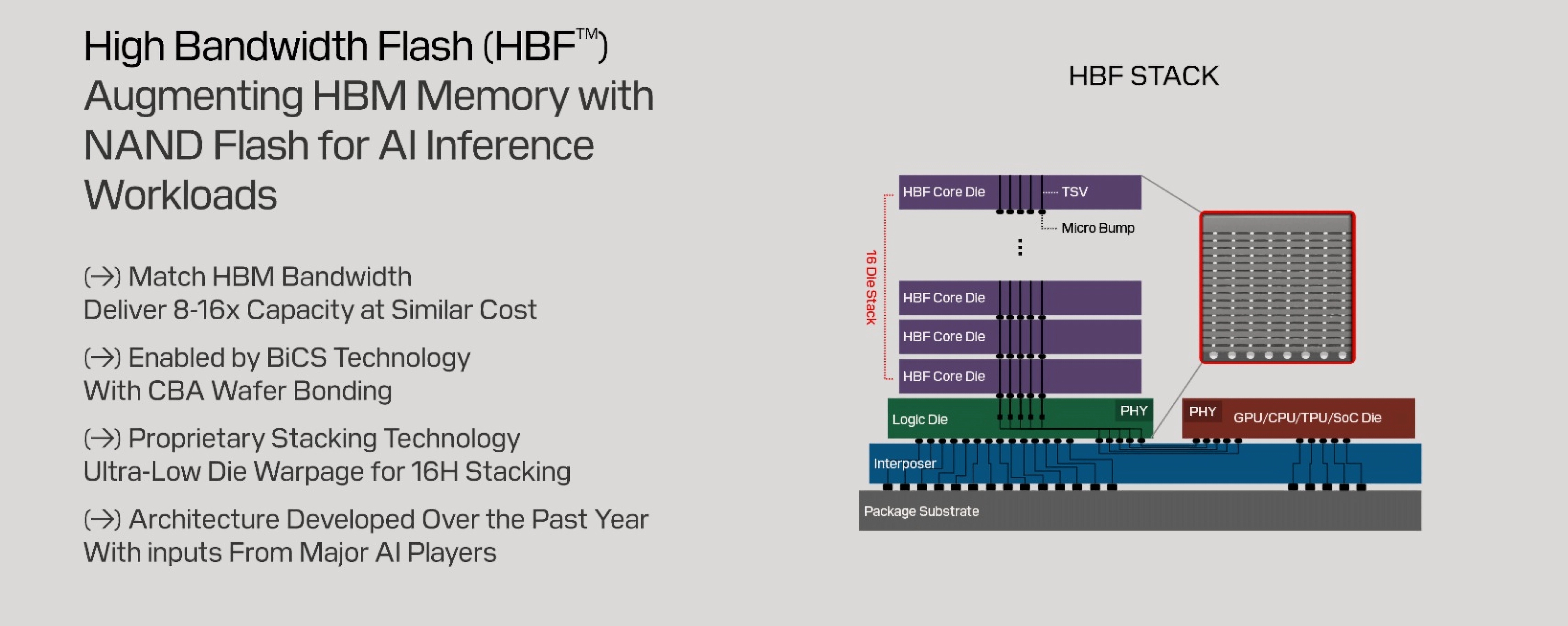
Notably, Sandisk plans to deliver HBF samples in 2H26, with first AI-inference devices expected by early 2027. Its first-generation HBF reportedly features 16-layer memory chips and offers up to 512GB per stack, aiming to match HBM’s bandwidth while boosting capacity by 8 to 16 times.
What is HBF?
According to eeNews Europe, citing Alper Ilkbahar, Sandisk’s Executive Vice President and Chief Technology Officer, HBF takes a different approach to NAND flash design. Instead of focusing on making chips smaller and cheaper like traditional methods, they optimized specifically for faster data transfer speeds, the report notes.
The report suggests SanDisk’s HBF breakthrough involves breaking down NAND memory arrays into numerous smaller sections that operate simultaneously. Using Kioxia’s BICS 3D-NAND technology, these mini arrays are stacked vertically, enabling Sandisk to create 16-layer memory chips that store 8 to 16 times more data than current HBM chips while maintaining similar costs, according to eeNews Europe.
As Sisa Journal points out, while HBM stacks DRAM chips to maximize memory bandwidth, HBF stacks 3D NAND arrays to dramatically increase parallel I/O operations.
SK hynix’s LPW NAND Also Under Development
It is worth noting that while teaming up with Sandisk on the development of HBF standards, SK hynix is reportedly working on another new type of NAND called Low Power Wide I/O (LPW) NAND, as per Sisa Journal.
According to sources cited by the report, SK hynix filed a trademark application for “LPW NAND” with the Korean Intellectual Property Office in early 2025. The new memory technology reportedly enhances processing speed by increasing I/O channels while reducing the speed per channel to lower power usage—a strategic move to meet the high-performance demands of AI inference applications, the report notes.
Read more
- [News] NAND Prices on the Rise: Micron and SanDisk Lead in April, with Samsung, SK hynix Likely to Follow
- [News] SanDisk to Raise NAND Prices Over 10% from April 1, Signaling Market Rebound
(Photo credit: Sandisk)
Please note that this article cites information from Sandisk, eeNews Europe and Sisa Journal.