


[News] SK hynix Breaks Ground on Indiana Packaging Plant, Eyes HBM4E by 3Q29; CEO Sees Tight Supply Through 2030

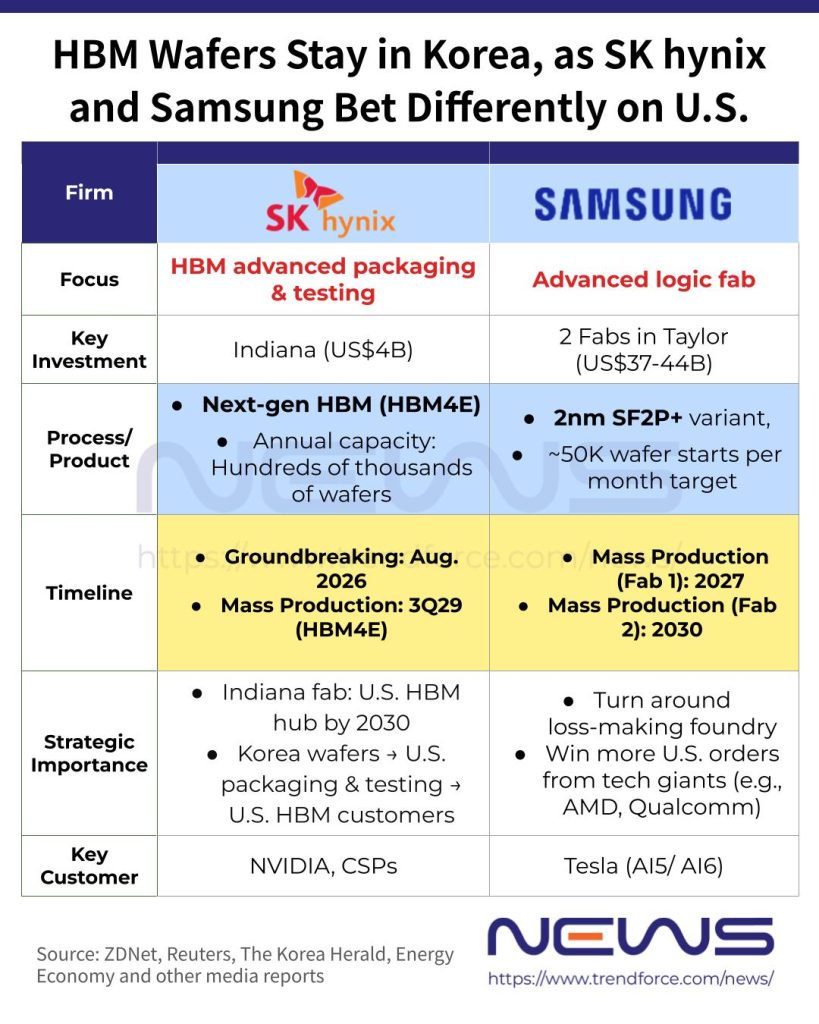
SK hynix broke ground on its first advanced semiconductor packaging plant in the U.S. on Aug. 27. The company aims to complete the cleanroom by October 2028, with ZDNet reporting that the facility is slated to begin HBM4E mass production in the third quarter of 2029.
According to Kyunghyang Shinmun, SK hynix’s Indiana fab will serve as a back-end production hub for stacking and packaging HBM and testing its performance. Advanced wafers produced in Korea will be shipped to the site for advanced packaging and testing before the finished HBM products are supplied to U.S. customers. It is expected to have an annual production capacity of several hundred thousand wafers, ZDNet adds.
The Elec notes that SK hynix will invest more than $4 billion (about 5.52 trillion won) in the facility. The U.S. Department of Commerce has also finalized $458 million in federal funding under the CHIPS Act.
Construction is now in the groundwork phase. SK hynix CEO Kwak Noh-Jung said the site is expected to become a key U.S. HBM production hub by 2030, The Elec reports.
Tight Memory Supply Seen Persisting Through 2030
Meanwhile, SK hynix expects tight memory supply to persist through the end of 2030, despite its aggressive capacity expansion, Newsis reports, citing CEO Kwak Noh-Jung. According to Kwak, there are currently no clear signs of a downturn, pointing to sustained supply constraints in the years ahead.
His view echoes earlier comments from SK Group Chairman Chey Tae-won. According to The Korea Herald, Chey said customers are seeking 60% to 100% more AI memory from SK hynix in 2027 than this year, warning that demand is likely to continue outpacing supply through 2027 despite ongoing capacity expansion.
Kioxia Expansion Puts SK hynix Ties in Focus
Meanwhile, SK hynix’s U.S. expansion comes as Japan’s Kioxia and U.S.-based Sandisk plan to invest more than $31 billion in Japan through 2032 to advance semiconductor technology and expand capacity. Kioxia will invest 1.8 trillion yen ($11.3 billion) to build a new memory chip facility at its Kitakami plant in northern Japan, Reuters reports.
The move also highlights SK hynix’s growing ties with Kioxia. Bain Capital’s special-purpose vehicle, BCPE Pangea Cayman2, has reportedly become Kioxia’s largest shareholder after Toshiba reduced its stake. The SPC now holds 14.19%, or 77.4 million shares, narrowly ahead of Toshiba’s 14.06%, according to ZDNet.
At SK hynix’s August 27 groundbreaking event, SK hynix CEO Kwak Noh-Jung said the company is considering closer cooperation with Kioxia, signaling potential deeper ties between the two memory chipmakers, as reported by Bloomberg and Kabutan.
Kwak said the company is “carefully considering how we can work together to develop the NAND flash memory market for the benefit of our customers and suppliers,” the reports note.
U.S. Tariff Pressure Drives Korean Chipmakers’ Expansion
SK hynix’s Indiana expansion comes as pressure mounts on South Korean chipmakers to deepen their U.S. manufacturing footprint, with Washington considering extending semiconductor tariffs to finished products, Energy Economy reports. The tariff threat is adding urgency to U.S. capacity expansion by the country’s leading chipmakers.
Samsung Electronics is likewise stepping up its Texas foundry buildout, with a planned $37 billion (about 51 trillion won) investment in Taylor. The report notes that Plant 1 is nearing completion and is targeting operations by year-end, with trial production potentially starting as early as September. Construction of Plant 2 is set to begin late this year, with mass production targeted for 2030, the report adds.
Read more
- [News] NVIDIA’s Reported 15% Server Hike Boosts Samsung, SK hynix, With HBM Prices Potentially Up 50%+ in 2027
- [News] Hot Chips 2026: Samsung’s zHBM Claims 70% Power-Efficiency Gain; SK hynix Evaluates Intel EMIB
(Photo credit: SK hynix)


