


[News] NVIDIA’s Supply Commitments Soar to $279B as Memory Costs Surge; New NVHBM Boosts Bandwidth 30%
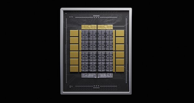
As NVIDIA forecasts a 70% surge in FY28 revenue, signaling that AI investment remains robust, the chipmaker is ramping up commitments to secure critical memory supply. According to Investopedia, NVIDIA’s supply and capacity commitments, as disclosed in Q2 FY27, jumped to $279 billion from $119 billion the prior quarter — driven largely by higher memory procurement.
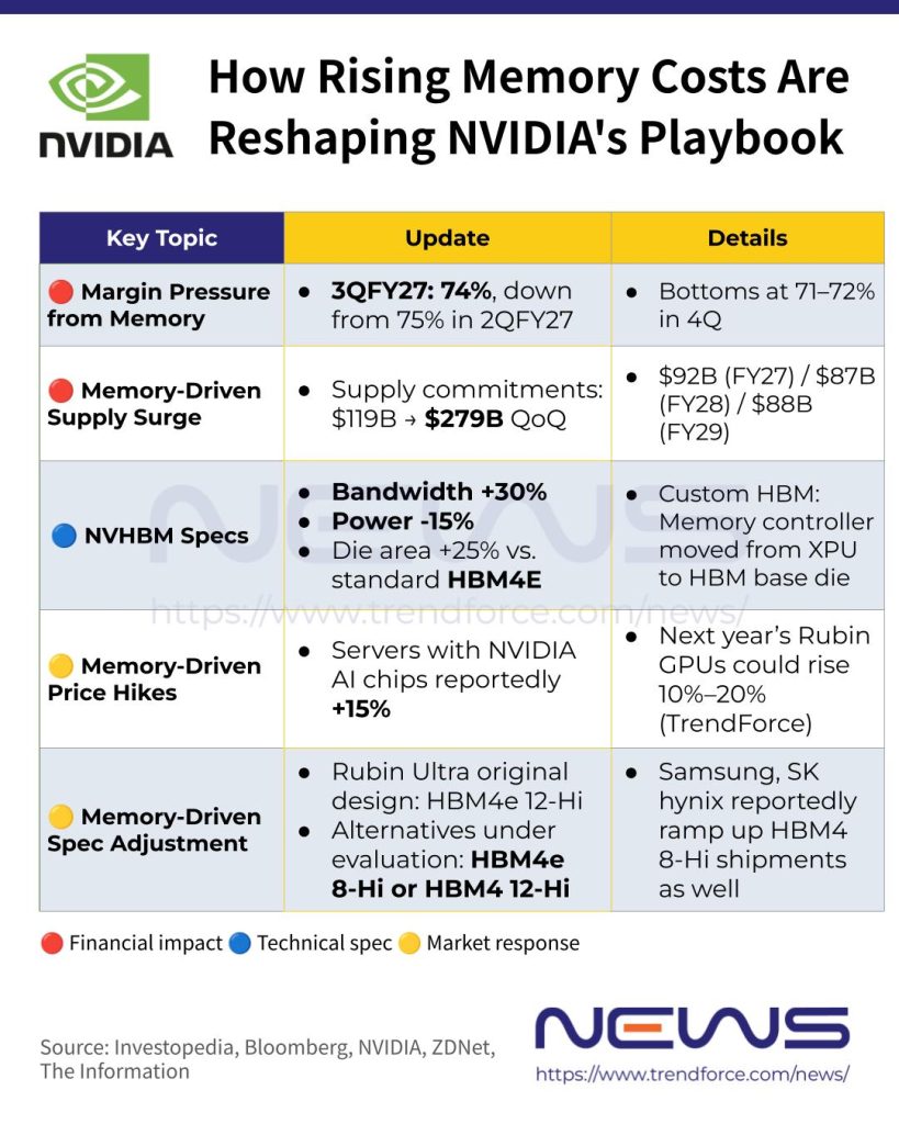
NVIDIA is also taking a more direct approach to the memory crunch, unveiling its custom HBM solution, NVHBM, which delivers up to 30% higher memory bandwidth while cutting HBM power consumption by 15%.
Memory Crunch to Persist Through 2028, Pressuring NVIDIA’s Margins
In the fiscal second-quarter, NVIDIA reports revenue of $96.2 billion, up 18% QoQ and 106% YoY, while adjusted EPS came in at $2.22, beating Wall Street estimates of $92.37 billion in revenue and $2.10 per share, Investopedia notes. Gross margin held at 75%, while the company forecast third-quarter revenue of $108 billion.
However, surging memory and component costs are set to weigh on profitability. Citing CFO Colette Kress, Reuters reports that gross margin is expected to slip to about 74% in Q3 and bottom at 71%–72% in Q4, below analysts’ 74.77% Q3 forecast.
The rising cost of memory is also driving a sharp increase in NVIDIA’s supply commitments. According to The Wall Street Journal, NVIDIA’s supply and capacity commitments, driven heavily by memory procurement, total $92 billion for the rest of FY27, followed by $87 billion in FY28 and $88 billion in FY29.
Despite its aggressive efforts to secure supply, NVIDIA expects the memory bottleneck to persist through at least FY2028, with Kress telling Investopedia that the AI boom will continue to strain supply as the company works to close the supply-demand gap.
NVHBM Moves the Memory Controller Into HBM to Unlock More Compute
Notably, as memory bandwidth becomes increasingly critical in the trillion-parameter era, NVIDIA is taking a more direct approach with its own custom HBM solution. As noted by Wccftech, NVHBM extends the company’s NVLink Fusion platform with a memory architecture aimed at boosting XPU performance while reducing power consumption.
NVIDIA explains that traditional HBM designs place the memory controller on the XPU die, taking up valuable silicon that could otherwise be used for compute. NVIDIA’s NVHBM takes a different approach, embedding its custom memory controller directly into the HBM base die using the same technology planned for future GPUs.
By moving the controller into the 3D HBM stack, NVHBM, according to NVIDIA, can deliver up to 30% higher memory bandwidth and 15% lower HBM power consumption, while freeing up to 25% more area on the XPU compute die versus standard HBM4E.
NVIDIA said that Amazon’s Annapurna Labs is among the first partners set to adopt the technology. The two companies will work on integrating NVHBM with NVIDIA’s NVLink scale-up architecture to improve performance and efficiency across AI workloads.
Looking ahead, Wccftech reports that AWS’s next-generation Trainium chips, starting with Trainium4, are expected to use NVLink Fusion to link NVIDIA GPUs with Amazon’s accelerators in a common rack-scale architecture. NVIDIA’s Feynman GPUs, due in 2028, could also become the first platform to adopt NVHBM, the report adds.
Read more
- [News] NVIDIA’s Reported 15% Server Hike Boosts Samsung, SK hynix, With HBM Prices Potentially Up 50%+ in 2027
- [News] NVIDIA Vera Rubin Spillover from HBM to NAND: CMX Fuels TLC Spot Price Rebound from June Dip
(Photo credit: NVIDIA)


