


[News] Chinese Advanced Packaging Firms Kicks-Start a New Round of Capacity Expansion
China is witnessing a fresh wave of investment in advanced semiconductor packaging, with a series of expansion projects targeting AI computing, automotive-grade chips, and next-generation memory technologies.
According to incomplete statistics, nearly ten major advanced packaging projects have been announced nationwide between May and July this year alone, with total disclosed investment approaching RMB 40 billion.
Billion-Yuan Investments Target High-End Heterogeneous Integration
Among projects focused on 2.5D/3D packaging and chiplet technologies, investment sizes are generally substantial, reflecting a clear shift toward high-density heterogeneous integration.
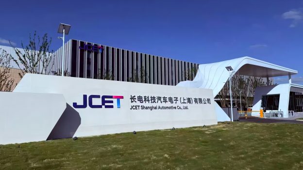
JCET to Invest RMB 7.8 Billion in Shanghai Lingang
On June 24, JCET announced plans to establish a new advanced packaging and testing facility in Shanghai’s Lingang area. The project carries a total investment of RMB 7.8 billion and will be developed in two phases, with Phase I expected to enter production in the second half of 2028.
The facility will feature production lines for high-density redistribution layers (RDL), ultra-fine-pitch bumping, large-format heterogeneous integration, and chiplet-based multi-die packaging, primarily serving AI servers, high-performance computing (HPC), and high-end GPUs.
Forehope Electronic Unveils RMB 10.3 Billion Packaging Base
Two days later, on June 26, Forehope Electronic announced plans to invest RMB 10.3 billion to build a high-end semiconductor packaging and testing base in Yuyao, Ningbo. Construction is scheduled over eight years.
The project will include four major production lines covering bumping, 2.5D integration, flip-chip (FC) packaging, and advanced wire-bond (WB) packaging, targeting AI edge processors, automotive control ICs, and high-end analog chips.
USC Technology Commits at Least RMB 7.5 Billion to HITS Packaging
On July 13, Shanghai Zhenglong Xinchuang Microelectronics, a subsidiary of Union Semiconductor (Hefei), launched its HITS advanced packaging R&D and commercialization project in Shanghai’s Jiading district.
With investment of no less than RMB 7.5 billion, the project will focus on three core technologies: ultra-fine-pitch bonding, high-density RDL, and large-area heterogeneous integration, targeting high-value applications including AI servers and HPC systems.
Automotive Packaging and Specialized Processes Gain Momentum
Expansion projects aimed at automotive semiconductors are showing a clear regional clustering trend, with new packaging facilities typically located alongside existing wafer fabrication plants or downstream automotive manufacturing hubs.
HKC Invests RMB 4 Billion in Shaoxing Packaging Facility
On July 17, HKC signed an agreement to build a RMB 4 billion advanced packaging and testing base in Shaoxing Binhai New Area. Upon completion of Phase I, the facility is expected to deliver a monthly capacity of 20 million 12-inch-equivalent packaged chips, focusing on automotive-grade devices and power analog ICs.
The project complements the region’s existing semiconductor ecosystem, which already includes UNT (formerly SMEC)’s large-scale automotive wafer manufacturing operations, strengthening Shaoxing’s vertically integrated automotive semiconductor supply chain.
Hotchip Technology and Mingtai Electronic Technology Expand in Southwest China
On July 16, Hotchip Technology signed an agreement to build a RMB 2 billion advanced packaging base in Nanchong, Sichuan. The facility will include wafer testing, bumping, and high-end COG/COF packaging lines to support compound semiconductor and industrial control applications.
Meanwhile, Mingtai Electronic completed the structural topping-out of Phase II of its Chengdu project in mid-July. Backed by RMB 500 million in investment, the expansion will add QFN, flip-chip, and system-in-package (SiP) production lines. Scheduled for completion in 2027, the project is expected to increase annual advanced packaging capacity by more than 10 billion devices.
Advanced Memory Packaging Enters a Rapid Growth Phase
As the industry seeks to overcome the “memory wall” limiting AI computing performance, packaging technologies for memory devices are increasingly shifting toward Fan-Out architectures and integrated memory-computing packaging.
Huatian Technology Advances RMB 3 Billion Nanjing Expansion
Between May and June, Huatian Technology accelerated the second-stage expansion of Phase II at its advanced packaging subsidiary in Nanjing, representing a RMB 3 billion investment.
The project is dedicated to advanced memory packaging and testing, focusing on Fan-Out packaging and reliability testing for SSD controllers and memory controller chips to support future production growth in high-end memory devices.
Biwin Storage Technology Launches RMB 1 Billion AI Memory Packaging Project
Leveraging the Greater Bay Area’s electronics manufacturing ecosystem, the facility will focus on Fan-Out packaging for memory chips and integrated memory-computing packaging technologies, targeting AI memory devices and high-end embedded memory products.
Taken together, these expansion projects point to three notable developments in China’s advanced packaging industry.
First, individual project sizes are growing significantly, with billion-yuan investments becoming increasingly common. Second, capacity additions are concentrated in leading-edge packaging technologies, particularly heterogeneous integration, chiplet architectures, Fan-Out packaging, and advanced flip-chip processes. Third, regional specialization is becoming more pronounced, as advanced packaging capacity is increasingly clustered around established wafer fabrication bases and downstream application ecosystems, reinforcing localized semiconductor supply chains.
(Photo credit: JCET)


