[News] Intel 18A Gains External Adopter Hitachi for Silicon Quantum Chip Project; 1,000-Qubit System Targeted for FY2030
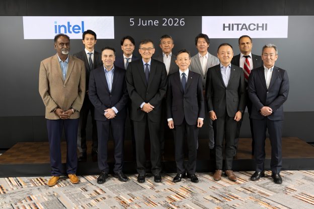
Intel’s 18A process has gained an early external adopter. According to a press release, Japan’s Hitachi has launched a silicon quantum computing collaboration with Intel K.K., Intel’s Japanese subsidiary, and AIST (the National Institute of Advanced Industrial Science and Technology). Under the partnership, Hitachi will co-develop qubit chips with Intel using the 18A process, aiming to establish the technologies needed to design and manufacture chips with 100 qubits or more and accelerate commercialization.
Building on the foundational technologies developed through the project, Hitachi aims to launch a cloud-based quantum computing service in fiscal 2027, followed by a phased rollout. The company also targets key milestones toward practical deployment, including a prototype silicon quantum computer with 100 qubits and quantum error correction in fiscal 2028, followed by a 1,000-qubit system in fiscal 2030.
The collaboration is part of NEDO’s “Accelerating the Development and Demonstration of Next-Generation Quantum Computers to Solve Social Challenges” R&D project. Under the initiative, Hitachi will conduct joint research with AIST through March 2029.
Leveraging Intel 18A for Silicon Quantum Computing
As noted by The Quantum Computing Report, silicon spin qubits offer a promising path to fault-tolerant quantum computing (FTQC) because they can leverage existing semiconductor manufacturing process and extreme ultraviolet (EUV) lithography. However, scaling from laboratory prototypes to fault-tolerant systems with millions of qubits requires overcoming device-to-device variability and wiring bottlenecks.
To address these challenges, Hitachi and Intel are pursuing four key development tracks. First, according to The Quantum Computing Report, Hitachi will design chips with more than 100 qubits using Intel’s 18A process and its quantum-device Process Design Kit (PDK), enabling standard foundry design rules while reducing device variability. They will also develop low-power cryogenic packaging and control circuits to reduce wiring complexity and thermal loads inside dilution refrigerators.
Hitachi also plans to develop high-density 3D integration technologies to connect qubit chips and control electronics at fine pitches, laying the foundation for systems with more than 1,000 qubits. Finally, as the report notes, the partners plan to build a cloud-accessible research platform at AIST’s G-QuAT, allowing external developers and researchers to run experimental workloads on silicon-qubit testbeds.
Beyond the quantum computing project, Intel and Hitachi have a broader strategic collaboration. According to Nikkei, the companies are applying Hitachi’s AI to semiconductor manufacturing to analyze production data, automate equipment maintenance, support physical AI for factory equipment, and improve chip production efficiency and yields.
Read more
- [News] Intel Pulls Forward 14A Timeline by One Year, Targeting 2028 Mass Production Near TSMC’s Roadmap
- [News] Intel Might Build Up to 90% of Nova Lake Compute Tiles on 18A, Scaling Back TSMC’s Planned Role
(Photo credit: Charlie Takeuchi on LinkedIn)