


[News] Chinese Team Achieved Major Breakthrough in Carbon Nanotube CFET Architecture

Complementary field-effect transistor (CFET) technology, which vertically stacks n-type and p-type FETs, is widely regarded as the key device architecture beyond FinFETs and gate-all-around (GAA) nanosheets for boosting logic density, shortening interconnects, and reducing cell footprint. The International Roadmap for Devices and Systems (IRDS) has identified CFET as a critical device for sub-2 nm technology nodes, with commercialization expected around 2032.
Recent presentations at IEDM and the VLSI Symposium from TSMC, imec, Samsung, and other research organizations have highlighted progresses in silicon nanosheet-based CFET technologies, including vertical stacking, sequential integration, dielectric isolation, contact engineering, and thermal budget control. These advances indicate that CFET development has moved beyond proof-of-concept toward manufacturing-oriented integration.
Two-dimensional semiconductors and carbon nanotubes are widely recognized as leading channel material candidates for the post-silicon era. While CFET devices and circuits based on 2D semiconductors and hybrid 2D/silicon integration have already demonstrated the promise of atomically thin channels, true carbon nanotube-based CFET devices and circuits have yet to be realized, despite carbon nanotubes offering high carrier mobility, low-temperature back-end process compatibility, and strong potential for three-dimensional integration.
A research team led by Xuelei Liang at Peking University’s School of Electronics has now developed the first all-carbon nanotube CFET digital logic circuits. To address the challenges of mismatched drive capability between p-type and n-type carbon nanotube transistors, as well as performance degradation caused by upper-layer fabrication, the researchers adopted a dopant-free CMOS approach and optimized the device architecture. The resulting top-layer n-FET and bottom-layer p-FET share an identical footprint while achieving highly balanced and closely matched electrical performance.
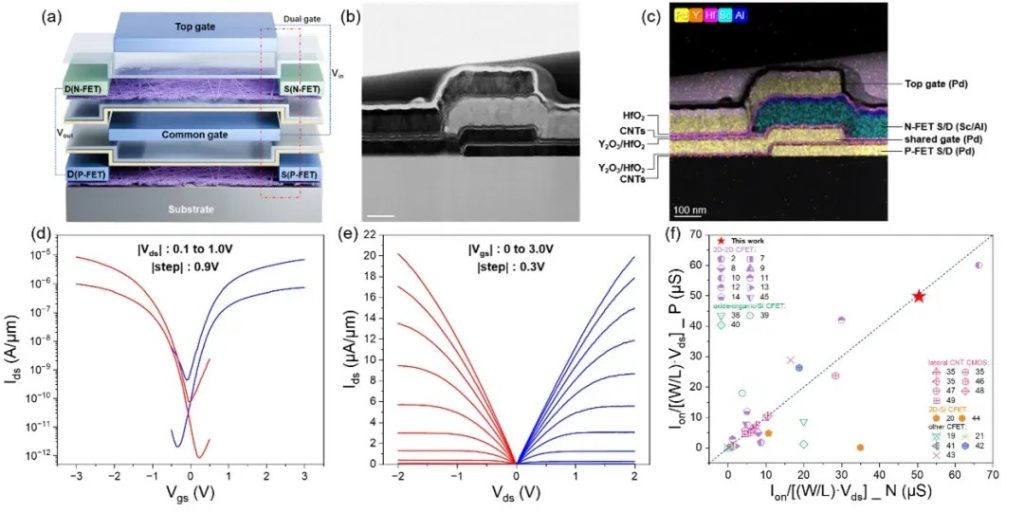
Figure 1. Structure of the carbon nanotube CFET device, showing the highly balanced and closely matched performance of the top-layer n-FET and bottom-layer p-FET.
(Credit: Peking University)
The fabricated CFET inverter demonstrated excellent rail-to-rail voltage transfer characteristics and low-power operation across a supply voltage range of 0.2–1.0 V. At 1.0 V, it achieved a peak voltage gain of 164, the highest reported for low-dimensional semiconductor CFET inverters. Benefiting from high device stability and a large noise margin of 61%–80% Vdd, the team further demonstrated NOR, OR, NAND, and AND gates, a four-transistor static random-access memory (4T-SRAM) cell, and the first five-stage ring oscillator based on an all-carbon nanotube CFET architecture.
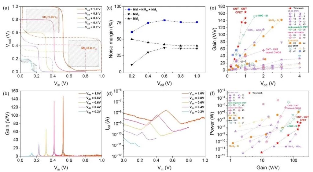
Figure 2. Performance of the carbon nanotube CFET inverter compared with previously reported CFET inverters.
(Credit: Peking University)
Leveraging the architecture’s intrinsic dual-layer carbon nanotube structure, the researchers also developed a three-dimensional stacked photodiode that improves light utilization while delivering an open-circuit photovoltage nearly twice that of a single-layer device, validating the additive gain enabled by 3D stacking. By directly coupling the photodiode output to the CFET inverter input, the team further demonstrated the first monolithically integrated three-dimensional carbon nanotube sensing-computing circuit. The prototype performs optical power and spectral sensing alongside logic processing across a broad wavelength range of 1,200–1,900 nm, achieving a minimum switching power of just 45 μW at 1,900 nm.
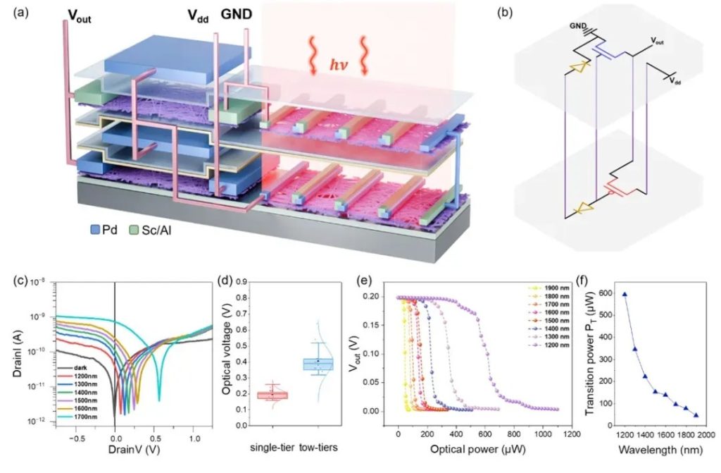
Figure 3. Monolithically integrated 3D sensing-computing circuit based on carbon nanotubes, demonstrating optical power and spectral sensing with integrated logic processing.
(Credit: Peking University)
The achievement fills a key gap in carbon nanotube CFET research and introduces a new technology path for high-density near-sensor and in-sensor computing architectures targeting future artificial intelligence and edge computing applications.
(Photo credit: FREEPIK)


