


[News] Huawei Expands Tau Scaling Law V2 Paper, Highlighting LogicFolding Path to Ascend AI Chips in 2030
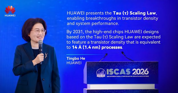
Two months after Huawei introduced the Tau (τ) Scaling Law in May, the company on July 3 disclosed additional details on an updated version, including further implementation insights and performance-related data. Notably, the V2 version of Time Scaling Theory for Multi-Level Electronic Systems (Tau Law) also outlines a roadmap extending LogicFolding beyond mobile SoCs into AI accelerators, including Huawei’s Ascend 990 expected around 2030.
Kirin 2026 Delivers Density Gain
In the near term, Kirin 2026 serves as the first validation platform for the dual-layer LogicFolding architecture. Chinese media outlets Guacha and mrjjxw.com, citing the paper published on ChinaXiv platform under the Chinese Academy of Sciences, report that compared with the 2025 Kirin 9030 Pro baseline, the Kirin 2026 achieves a transistor density increase from 155 MTr/mm² to 238 MTr/mm², representing a gain of approximately 53.5%.
The paper, cited by Guacha, also notes that achieving a similar gain through conventional geometric scaling would typically require about three years. As reported by Stdaily, Huawei’s first smartphone powered by the Kirin 2026 processor is expected to debut this fall, marking the first real-world test of the technology in the market.
According to Huawei, LogicFolding is a methodology that partitions digital, analog, and memory circuits across vertically stacked active tiers. On a mobile SoC, LogicFolding delivers a 55% stepwise increase in transistor density and a 41% reduction in power consumption at equivalent performance at a fixed device node, the company notes.
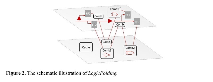
(Credit: Huawei)
Guacha further cites the V2 version of Time Scaling Theory for Multi-Level Electronic Systems (Tau Law), which projects logic folding will evolve from localized critical-path optimization to full multi-layer architectures over the next decade, with each package integrating three or more active layers.
The shift, according to the report, is driven by low-temperature hybrid bonding, which relaxes inter-layer thermal constraints, and TSV landing point migration from upper metals to M6, freeing over 30% of routing resources. Under this trajectory, transistor density is projected to scale toward 400 MTr/mm² and beyond between 2026 and 2035, the report suggests.
Next Phase: LogicFolding in Ascend AI Chips
Notably, the V2 version of Time Scaling Theory for Multi-Level Electronic Systems identifies Huawei’s Ascend AI chips as the next application of LogicFolding. According to Guacha, while the technology could enable Kirin processors to boost CPU clock speeds toward 4GHz and beyond, it is also expected to extend to the Ascend 990 AI accelerator around 2030. The report further notes that 3D folding is expected to become the primary carrier of the α architecture through 2035.
According to Huawei, in AI system designs, a co-designed stack—combining memory-semantic Unified Bus fabric, near-package Hi-ONE optical I/O, and edge-to-surface 3D folding—is projected to deliver more than 100× growth in hardware integration by 2035.
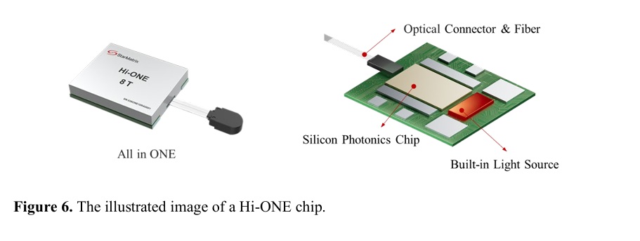
(Credit: Huawei)
Read more
- [News] Huawei, Xiaomi Reportedly Plan HBM-Inspired LLW DRAM for 2H27 to Boost On-Device AI in Smartphones
- [News] NVIDIA Jensen Huang Calls Huawei’s Tau Scaling Law a Breakthrough, But Sees No Challenge to TSMC
(Photo credit: Huawei)


