[News] NVIDIA Jensen Huang Calls Huawei’s Tau Scaling Law a Breakthrough, But Sees No Challenge to TSMC
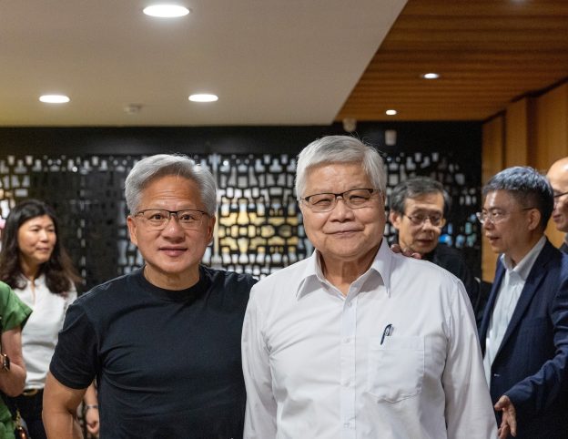
Huawei’s Tau (τ) Scaling Law is attracting growing industry attention as the company pursues a different path toward advancing chip performance. According to TechNews, NVIDIA CEO Jensen Huang commented on Huawei’s newly proposed semiconductor principle, the Tau (τ) Scaling Law, on May 28 during his visit to Taiwan. Huang described it as a breakthrough for Huawei, but said it does not represent a threat to TSMC.
On the matter, the report notes that Huang said Huawei’s Tau (τ) Scaling Law can boost chip performance through technologies such as chiplet stacking and hybrid bonding, enabling transistor counts to double, triple, or even quadruple without further shrinking the transistors. He described it as a promising technological approach.
However, Huang emphasized that TSMC has been developing related technologies for many years and already possesses highly advanced capabilities in this area. As the report adds, TSMC’s work on technologies including die stacking, 3D packaging, and hybrid bonding dates back nearly a decade.
TSMC has continued to strengthen its position in CoWoS, SoIC, and advanced packaging in recent years. The report adds that NVIDIA’s Blackwell and Rubin platforms, along with chips from AMD and Apple, rely heavily on TSMC’s advanced packaging capabilities.
Huawei’s LogicFolding Strategy Moves Toward Products, but Challenges Remain
As noted by Chosun Biz, a key pillar of Huawei’s Tau (τ) Scaling Law is LogicFolding, a technology that stacks circuits into two layers to shorten wiring paths and reduce signal latency. Unlike conventional planar chip designs, the approach aims to deliver 2nm- and 1nm-class performance without relying on advanced processes.
The technology is reportedly beginning to appear in Huawei’s product roadmap. Mydrivers notes that Huawei’s next-generation Kirin 2026 chip, expected to launch in autumn 2026, could become the world’s first commercial chip to adopt LogicFolding technology. Meanwhile, South China Morning Post reports that Huawei aims to develop chips by 2031 with performance comparable to 1.4nm technology, without relying on Western chipmaking tools restricted under export controls.
Still, the approach may face significant challenges. Chosun Daily reports that heat dissipation remains a key hurdle, while the added complexity of folding and stacking chips could substantially increase post-processing requirements. As a result, the feasibility of mass production remains uncertain.
Read more
- [News] Huawei Unveils New Semiconductor Principle – Tau (τ) Scaling Law
- [News] Peking Univ. Unveils EDA for Huawei LogicFolding; Kirin 2026 Reportedly Eyes 3nm-Class Performance
(Photo credit: NVIDIA Newsroom on X)