[News] Intel Reportedly Breaks Ground on Santa Clara Expansion for Next-Gen EUV Mask Capacity
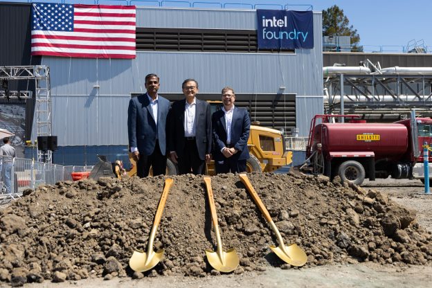
As interest in Intel’s foundry services continues to grow among a broader range of tech giants like Apple and NVIDIA, the chipmaker is accelerating its U.S. manufacturing buildout. According to Wccftech, Intel has officially broken ground on the latest expansion of its Santa Clara, California campus, with CEO Lip-Bu Tan and other senior executives attending the ceremony.
The expansion project was originally scheduled to begin in mid-2026, with the latest groundbreaking indicating that the timeline remains on track, the report adds.
Separately, policy timing could add further pressure to the buildout schedule, with a previous Tom’s Hardware report noting that semiconductor and advanced manufacturing projects must break ground by December 31, 2026, to qualify for the 35% Investment Tax Credit, and that projects initiated in 2027 or later will no longer be eligible for the incentive.
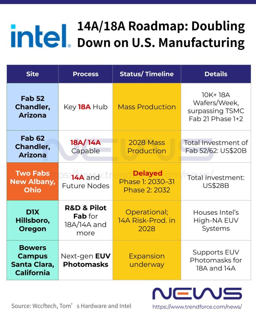
According to the San Francisco Business Times, Intel’s Santa Clara Bowers Campus development spans a 107,000-square-foot site and will include two three-story buildings dedicated to manufacturing, fabrication, and central utility operations. Wccftech adds that the site will support the production of EUV photomasks (reticles) critical to next-generation process nodes, including 18A-P and 14A.
Intel’s U.S. Expansion Roadmap in Focus
As Intel ramps up its 18A and 14A efforts, Fab 52 at the company’s Ocotillo campus in Chandler is set to serve as a key manufacturing backbone, according to Tom’s Hardware. The facility entered full-scale production in October 2025 as Intel’s first high-volume 18A site, initially producing Panther Lake compute tiles before expanding to Clearwater Forest later this year.
Notably, the report, citing CNBC, also highlights that Fab 52 is designed to support more than 10,000 Intel 18A wafer starts per week. At full ramp, this reportedly translates to roughly 40,000 wafer starts per month—exceeding the combined output of TSMC’s Fab 21 Phase 1 and Phase 2 in Arizona.
The next major Arizona expansion phase would be Fab 62, which is expected to enter production around 2028, according to Tom’s Hardware. While Intel has not disclosed its process node, Fab 62 is expected to provide flexibility to support either 14A production if Ohio falls behind schedule, or additional 18A capacity should demand outpace expectations, the report suggests.
Against this backdrop, Ohio, meanwhile, remains the most delayed project in Intel’s pipeline. After breaking ground in 2022 on a US$28 billion investment, the company has pushed Phase 1 completion to 2030 with operations in 2030–2031, followed by Phase 2 production in 2032.
Read more
- [News] Apple A22 Pro May Adopt 1.4nm in 2028; TSMC Remains Primary Supplier, Intel Reportedly Considered
- [News] Intel 18A-P Enters Risk Production, Targets 9% Performance Gain With Potentially Shortened Ramp
(Photo credit: Intel)


